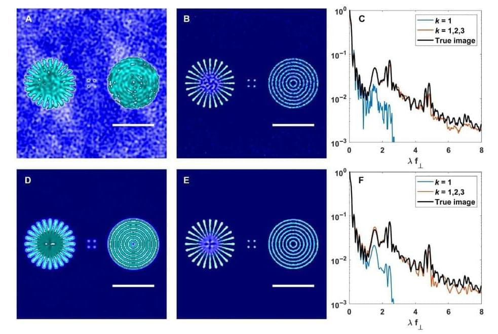
Toggle light / dark theme

This will help ensure that SSDs don’t suddenly just stop working one day. 😃 At least you get to back up your data.

It’s only available for data centers for now though. In the future, we may get our own when they perfect the technology.


If a NAND chip fails, these new SSDs detect it, move the data somewhere else on the drive, and keep on functioning.

Digital data storage is a growing need for our society and finding alternative solutions than those based on silicon or magnetic tapes is a challenge in the era of “big data.” The recent development of polymers that can store information at the molecular level has opened up new opportunities for ultrahigh density data storage, long-term archival, anticounterfeiting systems, and molecular cryptography. However, synthetic informational polymers are so far only deciphered by tandem mass spectrometry. In comparison, nanopore technology can be faster, cheaper, nondestructive and provide detection at the single-molecule level; moreover, it can be massively parallelized and miniaturized in portable devices. Here, we demonstrate the ability of engineered aerolysin nanopores to accurately read, with single-bit resolution, the digital information encoded in tailored informational polymers alone and in mixed samples, without compromising information density. These findings open promising possibilities to develop writing-reading technologies to process digital data using a biological-inspired platform.

DNA has evolved to store genetic information in living systems; therefore, it was naturally proposed to be similarly used as a support for data storage (1–3), given its high-information density and long-term storage with respect to existing technologies based on silicon and magnetic tapes. Alternatively, synthetic informational polymers have also been described (5–9) as a promising approach allowing digital storage. In these polymers, information is stored in a controlled monomer sequence, a strategy that is also used by nature in genetic material. In both cases, single-molecule data writing is achieved mainly by stepwise chemical synthesis (3, 10, 11), although enzymatic approaches have also been reported (12). While most of the progress in this area has been made with DNA, which was an obvious starting choice, the molecular structure of DNA is set by biological function, and therefore, there is little space for optimization and innovation.

Quantum computer: One of the obstacles for progress in the quest for a working quantum computer has been that the working devices that go into a quantum computer and perform the actual calculations, the qubits, have hitherto been made by universities and in small numbers. But in recent years, a pan-European collaboration, in partnership with French microelectronics leader CEA-Leti, has been exploring everyday transistors—that are present in billions in all our mobile phones—for their use as qubits. The French company Leti makes giant wafers full of devices, and, after measuring, researchers at the Niels Bohr Institute, University of Copenhagen, have found these industrially produced devices to be suitable as a qubit platform capable of moving to the second dimension, a significant step for a working quantum computer. The result is now published in Nature Communications.

Quantum dots in two dimensional array is a leap ahead

One of the key features of the devices is the two-dimensional array of quantum dots. Or more precisely, a two by two lattice of quantum dots. “What we have shown is that we can realize single electron control in every single one of these quantum dots. This is very important for the development of a , because one of the possible ways of making qubits is to use the spin of a single electron. So reaching this goal of controlling the single electrons and doing it in a 2-D array of was very important for us”, says Fabio Ansaloni, former Ph.D. student, now postdoc at center for Quantum Devices, NBI.

A viable quantum internet—a network in which information stored in qubits is shared over long distances through entanglement—would transform the fields of data storage, precision sensing and computing, ushering in a new era of communication.

This month, scientists at Fermi National Accelerator Laboratory—a U.S. Department of Energy national laboratory affiliated with the University of Chicago—along with partners at five institutions took a significant step in the direction of realizing a .

In a paper published in PRX Quantum, the team presents for the first time a demonstration of a sustained, long-distance teleportation of qubits made of photons (particles of light) with fidelity greater than 90%.

Researchers in Switzerland have found a new organic light emitting diode (OLED) material that could scale the technology up to inexpensively light entire rooms and homes for the first time. The results come from a new arrangement of copper electrons, CuPCP, that replaces more costly precious metal diodes (PHOLEDs). Let’s have some alphabet soup and learn about OLEDs.

Scientists at Lehigh University are developing a tiny generating plant, housed on a silicon chip, that they believe can produce enough hydrogen to run power-consuming portable devices.

The amount of hydrogen produced was small, but it was enough to demonstrate that the Lehigh project is feasible. Given time the Lehigh group believes they will develop a working generating plant, housed on a silicon chip that produces sufficient quantities of hydrogen to run different types of power consuming portable devices.

‘About 10 years ago people starting thinking: ‘can we take the same fabrication methods for silicon chips and instead of using them for electronics, use them for something else? said Mayuresh Kothare, assistant professor of chemical engineering.

I saw an ad for a tiny chip 1 that provides 5 volts 2 of isolated power: You feed 5 volts in one side, and get 5 volts out the other side. What makes this remarkable is that the two sides can have up to 5000 volts between them. This chip contains a DC-DC converter and a tiny isolation transformer so there’s no direct electrical connection from one side to the other. I was amazed that they could fit all this into a package smaller than your fingernail, so I decided to take a look inside.

I obtained a sample chip from Texas Instruments. Robert Baruch of project5474 decapped this chip for me by boiling it in sulfuric acid at 210 °C. This dissolved the epoxy package, leaving a pile of tiny components, shown below with a penny for scale. At the top are two tiny silicon dies, one for the primary circuitry and one for the secondary. Below the dies are two magnetized ferrite plates from the transformer. To the right is one of five pieces of woven glass fiber. At the bottom is a copper heat sink, partially dissolved by the decapping process. 3.

No escape.


Checking your notifications on a dive or live-streaming from the reef may not be such a far-off reality thanks to an underwater internet dubbed “Aqua-Fi.”

Developed by researchers at the King Abdullah University of Science and Technology (KAUST) in Thuwal, Saudi Arabia, Aqua-Fi uses a combination of lasers and existing computing technology to connect devices to the internet more than 30 feet underwater.

With the new technology, researchers were able to place a brief Skype call from a waterproof smartphone, using a standard Wi-Fi signal to connect to an underwater modem.

Researchers at Chalmers University of Technology, Sweden, have now shown that they can solve a small part of a real logistics problem with their small, but well-functioning quantum computer.

Quantum computers have already managed to surpass ordinary computers in solving certain tasks – unfortunately, totally useless ones. The next milestone is to get them to do useful things. Researchers at Chalmers University of Technology, Sweden, have now shown that they can solve a small part of a real logistics problem with their small, but well-functioning quantum computer.