Pigs with human kidneys? Brain-powered computer chips? Science is creating new kinds of living things – and our moral understanding needs to catch up fast.

Summary: New research delves into the distinctive human trait of sequential memory, setting us apart from bonobos. A recent study has also highlighted the joy in chasing passions over accomplishments. Groundbreaking discoveries show the human brain’s computational prowess, mirroring high-powered computers.
Additionally, the footprint of Big Tobacco is evident in the modern American diet through the promotion of hyperpalatable foods. Lastly, understanding the range of mind’s visualization abilities, from hyperphantasia to aphantasia, opens avenues for innovative treatments.

Quantum computing has provided new insights into a fundamental aspect of photochemical reactions that has previously proven difficult to study. The findings could improve scientists’ understanding of light-driven processes such as photosynthesis, smog formation and ozone destruction.
Photochemical processes occur when atomic nuclei and their electrons take on different configurations after absorbing a photon. Some of these reactions are guided by a quantum phenomenon called a conical intersection, where the potential energy surfaces that describe a molecule in its ground state and in its excited state converge. In these situations, quantum mechanical interference can prevent certain molecular transformations from taking place – a constraint known as a geometric phase. This limits the path that the reaction can take and affects the reaction outcome. The geometric phase has been known about since the 1950s, but due to the femtosecond timescales involved, it has never been directly observed in a molecular system.
Retention is an alternative to Attention in Transformers that can both be written in a parallel and in a recurrent fashion. This means the architecture achieves training parallelism while maintaining low-cost inference. Experiments in the paper look very promising.
OUTLINE:
0:00 — Intro.
2:40 — The impossible triangle.
6:55 — Parallel vs sequential.
15:35 — Retention mechanism.
21:00 — Chunkwise and multi-scale retention.
24:10 — Comparison to other architectures.
26:30 — Experimental evaluation.
Paper: https://arxiv.org/abs/2307.
Abstract:
In this work, we propose Retentive Network (RetNet) as a foundation architecture for large language models, simultaneously achieving training parallelism, low-cost inference, and good performance. We theoretically derive the connection between recurrence and attention. Then we propose the retention mechanism for sequence modeling, which supports three computation paradigms, i.e., parallel, recurrent, and chunkwise recurrent. Specifically, the parallel representation allows for training parallelism. The recurrent representation enables low-cost O inference, which improves decoding throughput, latency, and GPU memory without sacrificing performance. The chunkwise recurrent representation facilitates efficient long-sequence modeling with linear complexity, where each chunk is encoded parallelly while recurrently summarizing the chunks. Experimental results on language modeling show that RetNet achieves favorable scaling results, parallel training, low-cost deployment, and efficient inference. The intriguing properties make RetNet a strong successor to Transformer for large language models. Code will be available at this https URL.
Authors: yutao sun, li dong, shaohan huang, shuming ma, yuqing xia, jilong xue, jianyong wang, furu wei.
Links:
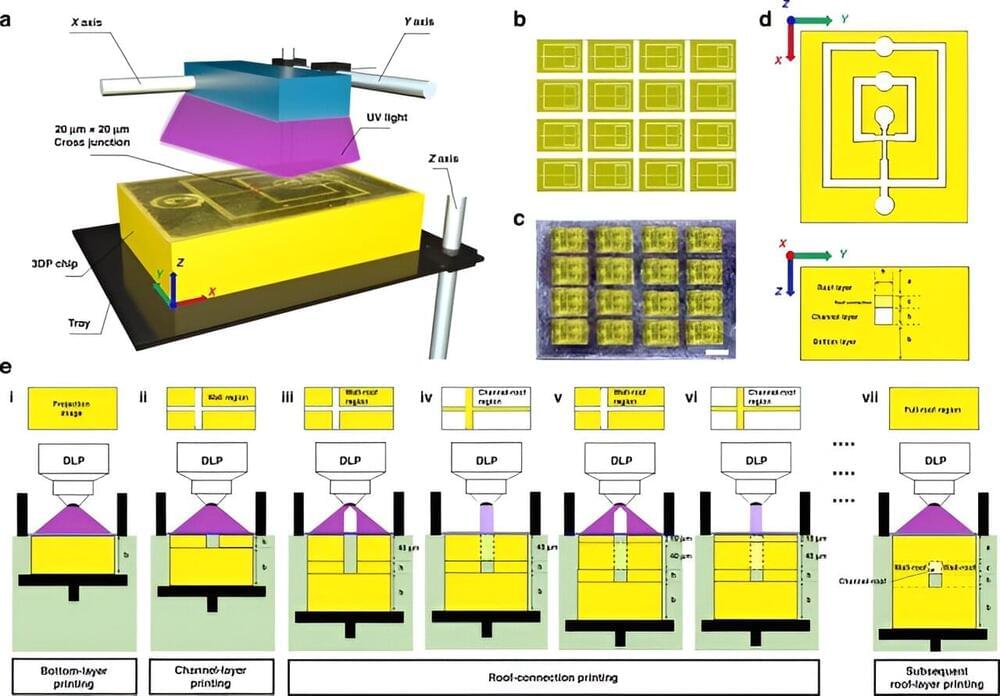
Conventional manufacturing methods such as soft lithography and hot embossing processes can be used to bioengineer microfluidic chips, albeit with limitations, including difficulty in preparing multilayered structures, cost-and labor-consuming fabrication processes as well as low productivity.
Materials scientists have introduced digital light processing as a cost-effective microfabrication approach to 3D print microfluidic chips, although the fabrication resolution of these microchannels are limited to a scale of sub-100 microns.
In a new report published in Microsystems and Nanoengineering, Zhuming Luo and a scientific team in biomedical engineering, and chemical engineering in China developed an innovative digital light processing method.
While semiconductor lithography gets the bulk of the attention in chipmaking, other processes are equally important in producing working integrated circuits (ICs). Case in point: packaging. An IC package provides the electrical, thermal, and mechanical transition from the semiconductor die or chip to the circuit board, which is often called a motherboard. One key element of the IC package is the substrate, which is essentially a miniature circuit board with copper traces that bonds to the input/output (I/O), power and ground pads on the chip and electrically connects these pads to the circuit board. The substrate provides a solid mechanical home for the chip and is also thermally matched to… More.
The release also quotes Babak Sabi, Intel senior vice president and general manager of Assembly and Test Development, who said: “After a decade of research, Intel has achieved industry-leading glass substrates for advanced packaging. We look forward to delivering these cutting-edge technologies that will benefit our key players and foundry customers for decades to come.”
Research into using glass substrates for chipmaking is nothing new. As Intel’s release says, the company has been working on this technology for at least a decade, as have other organizations such as the 3D Systems Packaging Research Center located at Georgia Tech, which was founded in 1994 – nearly 30 years ago. Last year, the Georgia Tech PRC launched an industry advisory board with Intel Fellow Ravi Mahajan as one of the initial board members. Intel has already spent more than a billion dollars to develop a glass-substrate manufacturing facility at its site in Chandler, Arizona.
So, if glass IC substrates are nothing new, why would Intel announce this particular development now, after ten years of corporate development and several years before these substrates find their way into products? On the technical side, it’s because existing ceramic and organic substrates are reaching the end of their ability to provide the electrical, thermal, and mechanical transitions for today’s most advanced semiconductors, which is doubly true as the industry adopts chiplets as an increasingly common way to put more transistors into a package.

A new record time for quantum coherence is reported, with a single-photon qubit encoded for 34 milliseconds. This is 55% longer than the previous record set in 2020.
In classical computing – such as the PC, smartphone, or other device you are currently using – information is processed with bits, which exist in a binary state of either a 0 or a 1. Quantum computing, by contrast, involves the processing of information with quantum bits, or qubits, which can exist in a “superposition” of both 0 and 1 simultaneously. This allows quantum computers to do certain types of calculations much faster than classical computers.
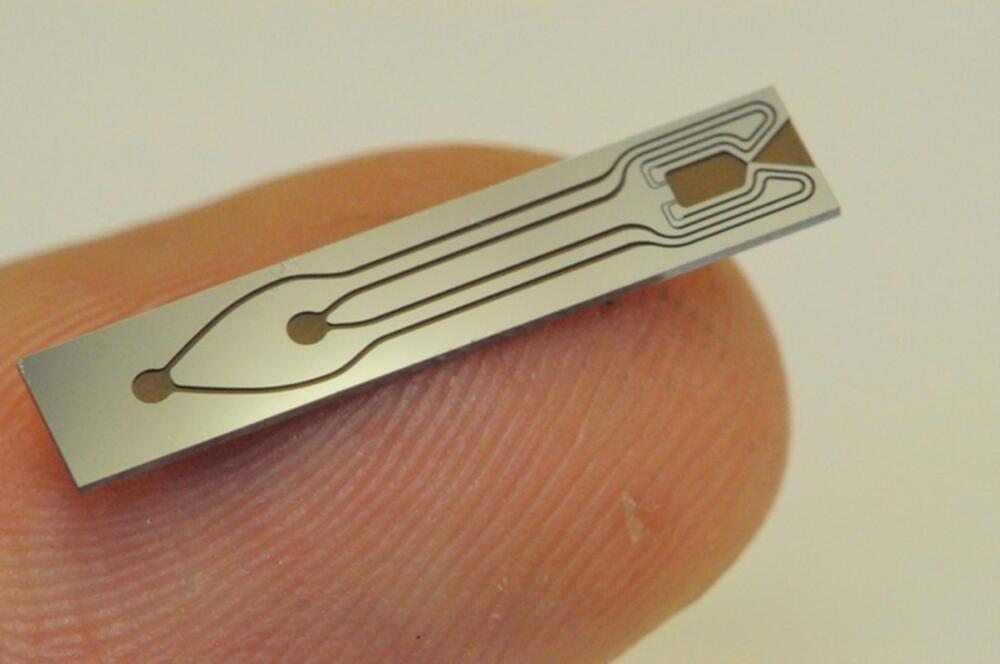
Designed to manoeuvre the smallest classes of satellite, the operation of this Iridium Catalysed Electrolysis CubeSat Thruster (ICE-Cube Thruster) developed with Imperial College in the UK is based on electrolysis.
This tiny fingernail-length space thruster chip runs on the greenest propellant of all: water.
Avoiding any need for bulky gaseous propellant storage, an associated electrolyser runs a 20-watt current through water to produce hydrogen and oxygen to propel the thruster.