Cordyceps computers? Mushroom Microchips? Penicillium Processors? Fungi, like the zombie fungus cordyceps, are full of complex electrical signaling, and tod…
Category: computing – Page 419
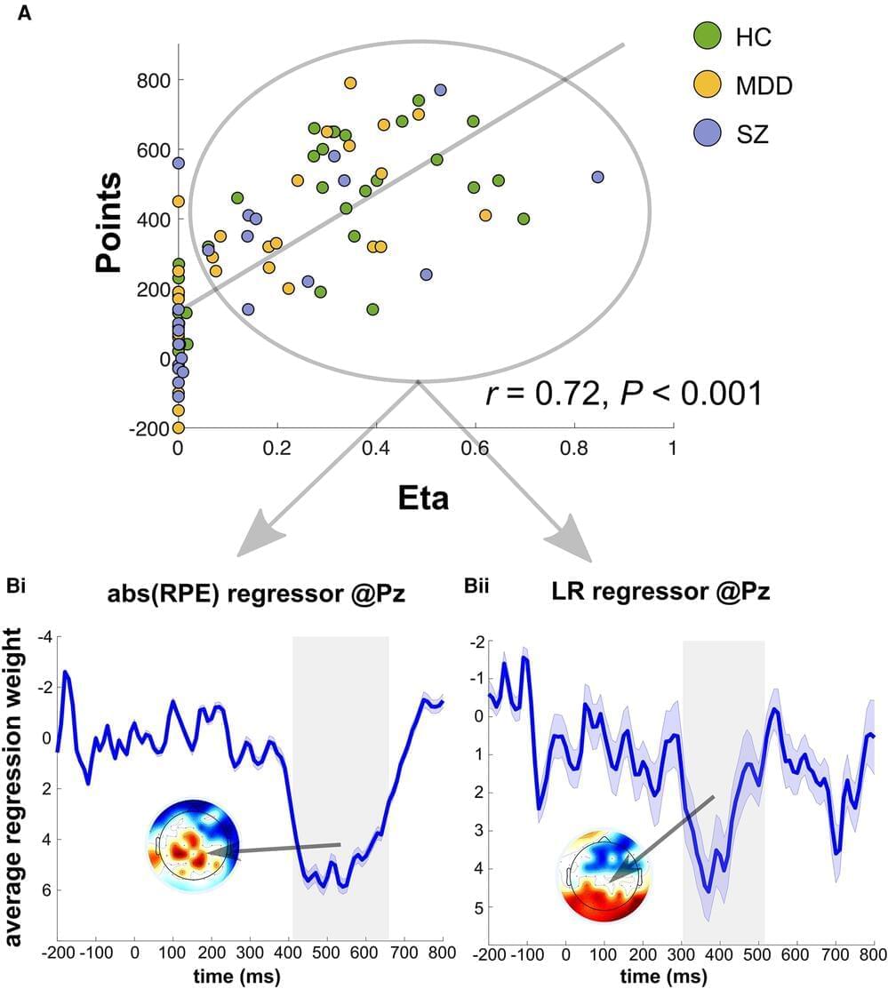
Why does depression cause difficulties with learning?
When learning, patients with schizophrenia or depression have difficulty making optimal use of information that is new to them. In the learning process, both groups of patients give greater weight to less important information and, as a result, make less than ideal decisions.
This was the finding of a several-months-long study conducted by a team led by neuroscientist Professor Dr. med. Markus Ullsperger from the Institute of Psychology at Otto von Guericke University Magdeburg in collaboration with colleagues from the University Clinic for Psychiatry & Psychotherapy and the German Center for Mental Health.
By using electroencephalography (EEG) and complex mathematical computer modeling, the team of researchers discovered that learning deficits in depressive and schizophrenic patients are caused by diminished/reduced flexibility in the use of new information.
First unhackable shopping transactions carried out on quantum internet
A secure exchange between a merchant and a buyer has been successfully tested as a proof of concept using a small quantum computing network in China.
This New Semiconductor Could Revolutionize Computing
Potentially good technology if it makes it to market. A new semiconductor would be great!
Researchers at the Georgia Institute for Technology have found a new semiconductor that’s a really good candidate for making computers faster and smaller than ever. Amazingly enough, it works by combining graphene with silicon carbide, to give a material with a sensible band gap that still has a high thermal conductivity.
Correction to what I say at 02:54 — That should have been voltage, not current.
Paper here: https://www.nature.com/articles/s4158…
🤓 Check out our new quiz app ➜ http://quizwithit.com/
China develops ‘Star Wars’-style deflector plasma shield to defend drones
According to Chinese news sources, Chinese scientists have allegedly harnessed plasma to develop a working energy shield for drones and other military tech.
Chinese scientists have allegedly developed an energy shield to protect some of its military assets, the South China Morning Post (SCMP) reports. Utilizing a special kind of plasma, the energy shield is designed to resist potentially harmful microwaves from damaging delicate electronics. If the claims of its existence are true, the new shield is a significant leap in directed energy technology, especially in the ongoing aerial-to-anti-aerial arms race.
Shields up!
High-powered electromagnetic radiation (EM), like microwaves, can compromise modern technology, including military chips fortified with special circuits, even at close range. These powerful waves can cause electrical interference in the chip and significantly increase its internal temperature. For this reason, sensitive electronics must be shielded and protected as much as possible.
Quantum Leap: The New Frontier of Polymer Simulations
A new study shows how quantum computing can be harnessed to discover new properties of polymer systems central to biology and material science.
The advent of quantum computing is opening previously unimaginable perspectives for solving problems deemed beyond the reach of conventional computers, from cryptography and pharmacology to the physical and chemical properties of molecules and materials. However, the computational capabilities of present-day quantum computers are still relatively limited. A newly published study in Science Advances fosters an unexpected alliance between the methods used in quantum and traditional computing.
The research team, formed by Cristian Micheletti and Francesco Slongo of SISSA in Trieste, Philipp Hauke of the University of Trento, and Pietro Faccioli of the University of Milano-Bicocca, used a mathematical approach called QUBO (from “Quadratic Unconstraint Binary Optimization”) that is ideally suited for specific quantum computers, called “quantum annealers.”

How To Use the Emacs Editor in Linux
Emacs is one of the oldest and most versatile text editors. The GNU Emacs version was originally written in 1984 and is well known for its powerful and rich editing features. It can be customized and extended with different modes, enabling it to be used like an Integrated Development Environment (IDE) for programming languages such as Java, C, and Python.
For those who have used both the Vi and the user-friendly nano text editors, Emacs presents itself as an in-between. Its strengths and features resemble those of Vi, while its menus, help files, and command-keys compare with nano.
In this article, you’ll learn how to install Emacs on an Ubuntu 22.04 server and use it for basic text editing.
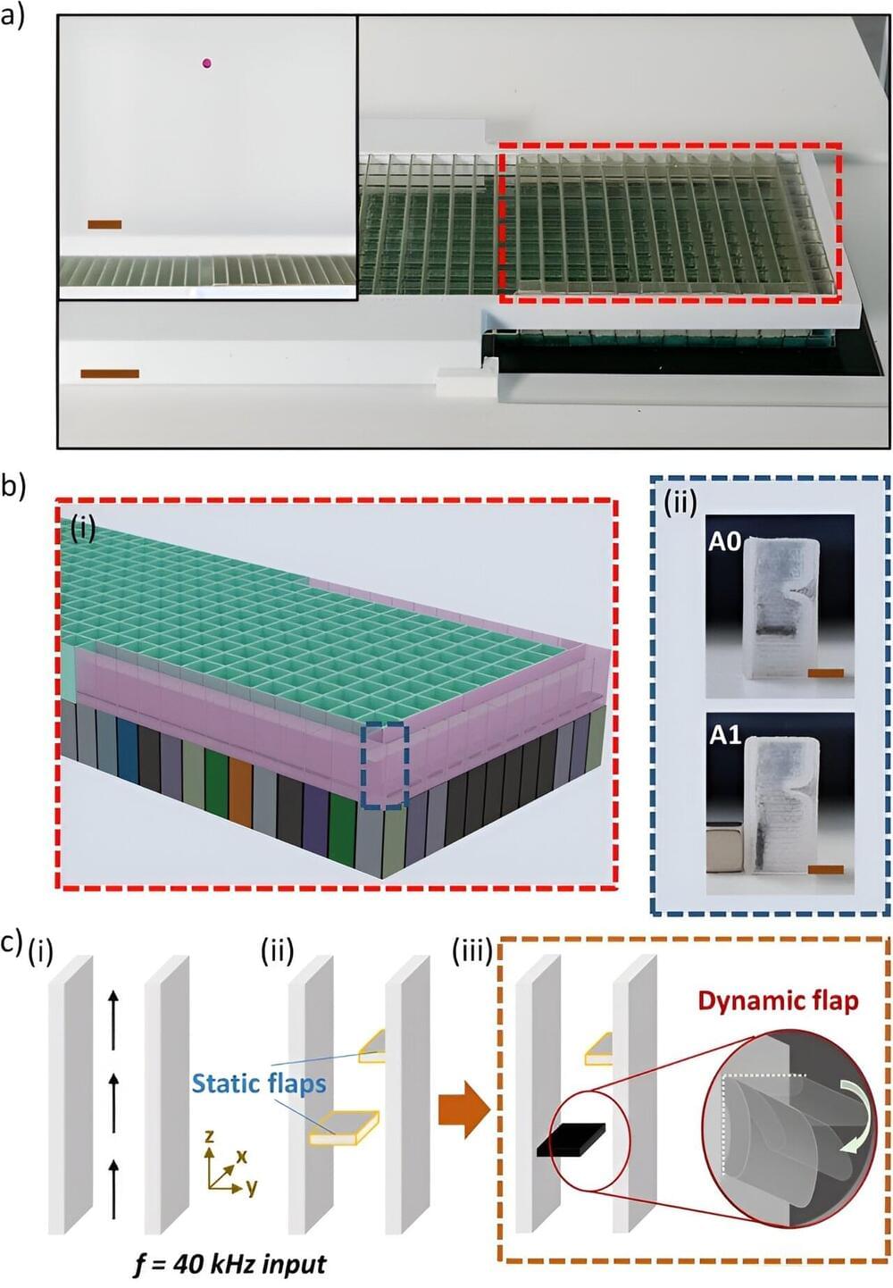
A magnetically actuated acoustic metamaterial
Space coiling acoustic metamaterials are static and require manual reconfiguration for sound-field modulation. In a new report published in Communications Materials, Christabel Choi, and a team of scientists in computer science and engineering in the U.K., and Italy, developed an approach for active reconfiguration with standalone dynamics to space-coil unit cells known as dynamic meta-bricks.
The meta-bricks housed an actuatable, magnetorheological, elastomeric flap, to function like a switch and to directly regulate the transmitted ultrasound. The scientists showed the synergy between active and passive reconfigurability to develop multifunctional metamaterials with additional degrees of freedom, for design and implementation.

MIT/Harvard spinout plans 10,000-qubit, error-corrected quantum computer by 2026
QuEra, a quantum computing startup founded by researchers from Harvard and the Massachusetts Institute of Technology, recently released what may be the most ambitious quantum technology roadmap we’ve seen yet.
The company plans on releasing a quantum computer with 100 logical qubits and 10,000 physical qubits by 2026. It also claims this planned system will demonstrate “practical quantum advantage,” meaning they’d be capable of useful computation feats that classical, binary computers aren’t.