Capgemini’s CEO says Europe’s dependency on semiconductor imports will remain ‘huge’ for years to come.

Quantum engineering, a dynamic discipline bridging the fundamentals of quantum mechanics and established engineering fields has developed significantly in the past few decades. Two-level systems such as superconducting quantum bits are the building blocks of quantum circuits. Qubits of this type are currently the most researched and used in quantum computing applications1,2,3,4,5. The characteristics of the superconducting qubits such as eigen energies, non-linearity, coupling strengths etc. can be tailored easily by adjusting the design parameters6,7. Qubits have large non-linearity, which makes it possible to selectively address and control them1,3,7,8. This dynamic property makes superconducting qubits a strong candidate for plethora of applications. Other two-level microscopic quantum systems9,10,11,12,13,14 also have certain advantages and may be used in the future.
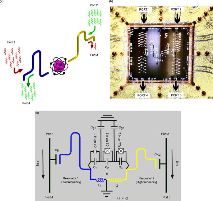
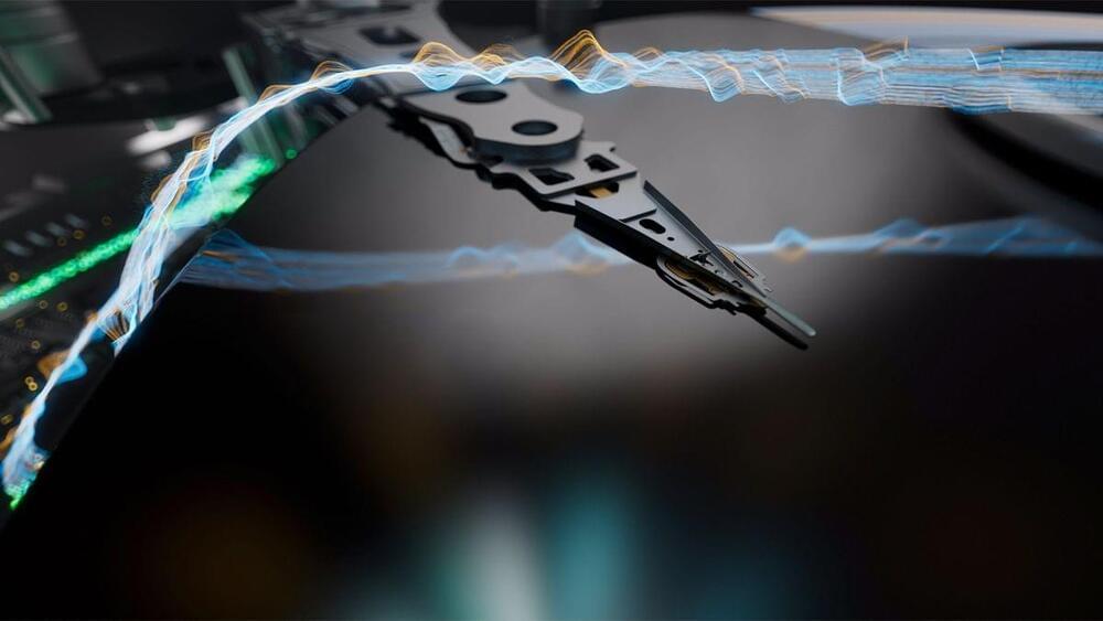
Quantum devices operate at low temperatures and require good isolation from external noises. Microwave devices, such as circulators and isolators, protect quantum circuits by unidirectionally routing the output signal, whilst simultaneously isolating noise from the output channel back to the quantum circuit. Their non-reciprocal character relies on the properties of ferrites15,16,17. Ferrite-based non-reciprocal devices are bulky15,16,17, and they cannot be positioned near the quantum circuit because they require strong magnetic fields. Although commercial ferrite based non-reciprocal devices harness high isolation and low insertion loss, their dependency on magnetic components limits the scalability of cryogenic quantum circuits15,16,18,19. Various ferrite-free approaches based on non-linear behavior of artificial atoms16, dc superconducting quantum interference devices (dc-SQUID)20,21, and arrays of Josephson junctions (JJ’s)19,22,23,24, have been experimentally demonstrated and implemented. Recently, a circuit based on semiconductor mixers has been used to realize a compact microwave isolator, which the authors claim could be extended to an on-chip device using Josephson mixers, although the “on-chip” demonstration is not yet reported25. Additionally, mesoscopic circulators exploiting the quantum Hall effect to break time-reversal symmetry of electrical transport in 2D systems are explored at a cost of larger magnetic fields deleterious to superconducting circuits18,26,27,28,29. More recently, a passive on-chip circulator based on three Josephson elements operating in charge-sensitive regime was demonstrated30. Such devices are frequently limited by their parameter regime, leaving them charge sensitive and therefore difficult to implement in a practical scenario. However, it is possible to mitigate the charge-sensitivity by carefully tuning the device parameters. Our device operates in a parameter regime that is not sensitive to charge fluctuations or charge parity switching, a fundamental requirement for any practical implementation, and requires small magnetic field. The reported device is a proof of concept (PoC), potentially useful in the applications relevant to microwave read-out components in the field of superconducting quantum circuits.
In this work, we present a robust and simple on-chip microwave diode demonstrating transmission rectification based on a superconducting flux qubit8. The concept of the device is shown in Fig. 1a. The flux qubit is inductively coupled to two superconducting resonators of different lengths with different coupling strengths. The design details are reported later in this section. Probing the qubit at the half-flux (degeneracy point) with one tone-spectroscopy, we observe identical patterns of transmission coefficient for signals propagating in the opposite directions, which are shifted by 5 dB in power. This shift indicates the non-reciprocal behaviour in our device, expressed in terms of transmission rectification ratio ® in this article. The origin of this effect is the non-linearity of the flux qubit, which controls the transmission coefficient of the whole structure.
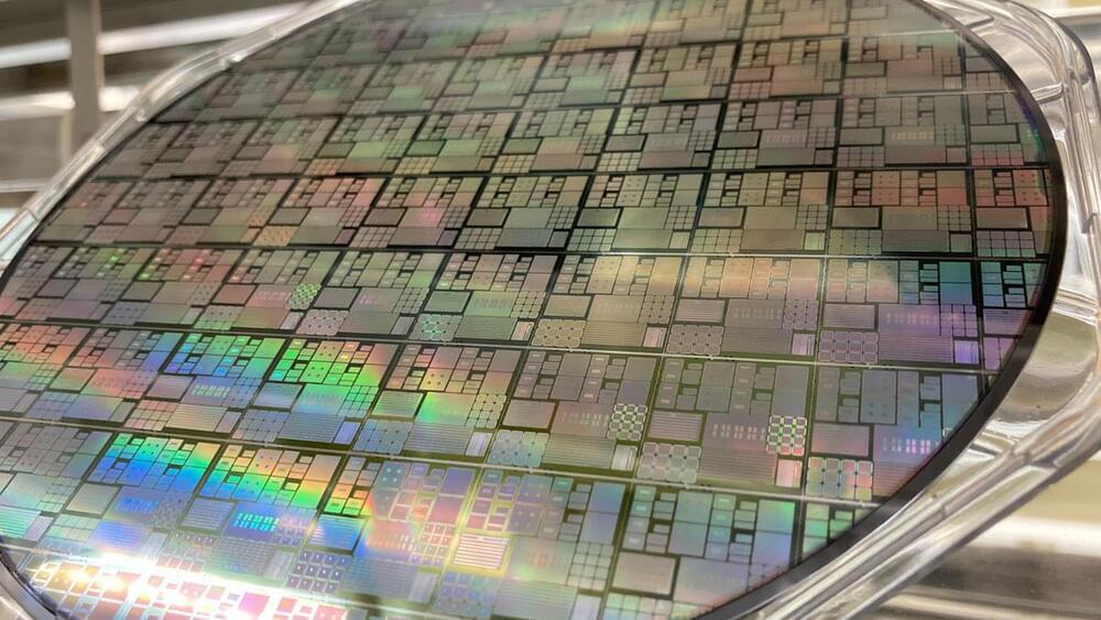
When Taiwan Semiconductor Manufacturing Co. (TSMC) is prepping to roll out an all-new process technology, it usually builds a new fab to meet demand of its alpha customers and then either adds capacity by upgrading existing fabs or building another facility. With N2 (2nm-class), the company seems to be taking a slightly different approach as it is already constructing two N2-capable fabs and is awaiting for a government approval for the third one.
We are also preparing our N2 volume production starting in 2025,” said Mark Liu, TSMC’s outgoing chairman, at the company’s earnings call with financial analysts and investors. “We plan to build multiple fabs or multiple phases of 2nm technologies in both Hsinchu and Kaohsiung science parks to support the strong structural demand from our customers. […] “In the Taichung Science Park, the government approval process is ongoing and is also on track.”
TSMC is gearing up to construct two fabrication plants capable of producing N2 chips in Taiwan. The first fab is planned to be located near Baoshan in Hsinchu County, neighboring its R1 research and development center, which was specifically build to develop N2 technology and its successor. This facility is expected to commence high-volume manufacturing (HVM) of 2nm chips in the latter half of 2025. The second N2-capable fabrication plant by is to be located in the Kaohsiung Science Park, part of the Southern Taiwan Science Park near Kaohsiung. The initiation of HVM at this plant is projected to be slightly later, likely around 2026.
Silicon carbide is becoming a major player on the quantum scene. Widely used in specialized electronics goods such as LEDs and electric vehicles, silicon carbide boasts versatility, wide commercial availability, and growing use in high-power electronics, making it an attractive material for quantum information science, whose impact is expected to be profound.
Drawing on physics at the atomic scale, technologies such as quantum computers, networks, and sensors will likely revolutionize areas as varied as communication, drug development, and logistics in the coming decades.
Now, scientists at the U.S. Department of Energy’s (DOE) Argonne National Laboratory, DOE’s Sandia National Laboratories, and partner institutions have conducted a comprehensive study on the creation of qubits—the fundamental units of quantum information processing—in silicon carbide.
When Mickael Perrin started out on his scientific career 12 years ago, he had no way of knowing he was conducting research in an area that would be attracting wide public interest only a few years later: Quantum electronics. “At the time, physicists were just starting to talk about the potential of quantum technologies and quantum computers,” he recalls.
“Today there are dozens of start-ups in this area, and governments and companies are investing billions in developing the technology further. We are now seeing the first applications in computer science, cryptography, communications and sensors.” Perrin’s research is opening up another field of application: Electricity production using quantum effects with almost zero energy loss. To achieve this, the 36-year-old scientist combines two usually separate disciplines of physics: thermodynamics and quantum mechanics.
In the past year, the quality of Perrin’s research and its potential for future applications has brought him two awards. He received not only one of the ERC Starting Grants that are so highly sought-after by young researchers, but also an Eccellenza Professorial Fellowship of the Swiss National Science Foundation (SNS)F. He now leads a research group of nine at Empa as well as being an Assistant Professor of Quantum Electronics at ETH Zurich.
In a recent study, a team of researchers at Max Planck Institute for Physics proposed that advanced extraterrestrial civilizations may be using black holes as quantum computers. No matter how advanced a civilization may be, we are all bound by the laws of quantum physics and gravity. So, if aliens are indeed out there, they could be using the geometry of spacetime around a black hole which behaves like a quantum computer. And, as if that weren’t enough, quantum computing is also immune to decryption, making it the perfect tool for secure communication. Roger Penrose, famously proposed that it is possible to extract limitless energy from a black hole by tapping into its Ergosphere. This is a region just outside the event horizon, where matter falling into the black hole forms a disk that spins at nearly the speed of light and emits massive amounts of radiation. Several researchers now suggest that this may be the ultimate power source for advanced civilizations. Subscribe to Science Time: https://www.youtube.com/sciencetime24 #science #shorts #space
Data is written to the memory cell by changing the magnetization in the free layer (which acts as the ‘storage’ layer in the MRAM bit cell) by passing a current through the heavy metal layer, which generates a spin current and injects it into the adjacent magnetic layer, switching its orientation and thus changing its state. Reading data involves assessing the magnetoresistance of the MTJ by directing a current through the junction. The main difference between STT-and SOT-MRAM resides in the current injection geometry used for the write process, and apparently, the SOT method ensures lower power consumption and device longevity.
While SOT-MRAM offers lower standby power than SRAM, it needs high currents for write operations, so its dynamic power consumption is still quite high. Furthermore, SOT-SRAM cells are still larger than SRAM cells, and they are harder to make. As a result, while the SOT-SRAM technology looks promising, it is unlikely that it will replace SRAM any time soon. Yet, for in-memory computing applications, SOT-MRAM could make a lot of sense, if not now, but when TSMC learns how to make SOT-MRAM cost-efficiently.

In a paper published in Science Jan. 18, scientists Chad Mirkin and Sharon Glotzer and their teams at Northwestern University and University of Michigan, respectively, present findings in nanotechnology that could impact the way advanced materials are made.
The paper describes a significant leap forward in assembling polyhedral nanoparticles. The researchers introduce and demonstrate the power of a novel synthetic strategy that expands possibilities in metamaterial design. These are the unusual materials that underpin “invisibility cloaks” and ultrahigh-speed optical computing systems.
“We manipulate macroscale materials in everyday life using our hands,” said Mirkin, the George B. Rathmann Professor of Chemistry at the Weinberg College of Arts and Sciences.