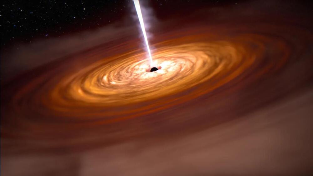
Toggle light / dark theme

While our attention is mostly directed towards ever smaller-integrated silicon circuits providing faster and faster computing, there’s another area of integrated electronics that operates at a much lower speed which we should be following. Thin-film flexible circuitry will provide novel ways to place electronics where a bulky or expensive circuit board with traditional components might be too expensive or inappropriate, and Wikichip is here to remind us of a Leuven university team who’ve created what is claimed to be the fastest thin-film flexible microprocessor yet. Some of you might find it familiar, it’s our old friend the 6502.

The choice of an archaic 8-bit processor might seem a strange one, but we can see the publicity advantage — after all, you’re reading about it here because of it being a 6502. Plus there’s the advantage of it being a relatively simple and well-understood architecture. It’s no match for the MHz clock speeds of the original with an upper limit of 71.4 kHz, but performance is not the most significant feature of flexible electronics. The production technology isn’t quite ready for the mainstream so we’re unlikely to be featuring flexible Commodore 64s any time soon, but the achievement is the impressive feat of a working thin-film flexible microprocessor.

Meanwhile, if you’re curious about the 6,502, we took a look at the life of its designer, [Chuck Peddle].

We have all had the experience of one of our electronic devices overheating. Needless, to say that when that happens, it becomes dangerous both for the device and its surroundings. But considering the speed at which devices work, is overheating avoidable?

A 740 percent increase in power per unit.

Researchers at the University of Illinois at Urbana-Champaign (UIUC) and the University of California, Berkeley (UC Berkeley) have recently devised an invention that could cool down electronics more efficiently than other alternative solutions and enable a 740 percent increase in power per unit, according to a press release by the institutions published Thursday.

Imec plots a course to 1nm chips, and beyond.


Imec, the most advanced semiconductor research firm in the world, recently shared its sub-‘1nm’ silicon and transistor roadmap at its Future Summit event in Antwerp, Belgium. The roadmap gives us a rough idea of the timelines through 2036 for the next major process nodes and transistor architectures the company will research and develop in its labs in cooperation with industry giants, like TSMC, Intel, Samsung, and ASML, among many others.

The roadmap includes breakthrough transistor designs that evolve from the standard FinFET transistors that will last until 3nm, to new Gate All Around (GAA) nanosheets and forksheet designs at 2nm and A7 (seven angstroms), respectively, followed by breakthrough designs like CFETs and atomic channels at A5 and A2. As a reminder, ten Angstroms are equal to 1nm, so Imec’s roadmap encompasses sub-‘1nm’ process nodes.

You might not have heard of the Interuniversity Microelectronics Centre (imec) before, but it ranks among the most important companies in the world, alongside better-known companies like TSMC and EUV-toolmaker ASML. Think of imec as a silicon Switzerland, of sorts. While the semiconductor research-focused imec doesn’t operate with much fanfare, it serves as the quiet cornerstone of the semiconductor industry, bringing fierce rivals like Intel, TSMC, and Samsung together with chip toolmakers such as ASML and Applied Materials, not to mention the equally-critical semiconductor software design companies (EDA) like Cadence and Synopsys, in a non-competitive environment. This collaboration allows the companies to work together to define the next generation of tools and software they will use to design and manufacture the chips that power the world.

Benjy WangProbably could be limited by a simulation restart.

Jim RohrichNo limits.

Omuterema Akhahenda shared a link.

PHYSICS:

Our electronics can no longer shrink and are on the verge of overheating. But in a new discovery from the University of Copenhagen, researchers have uncovered a fundamental property of magnetism, which may become relevant for the development of a new generation of more powerful and less hot computers.

From TVs, to solar cells, to cutting-edge cancer treatments, quantum dots are beginning to exhibit their unique potential in many fields, but manufacturing them at scale would raise some issues concerning the environment. Scientists at Japan’s Hiroshima University have demonstrated a greener path forward in this area, by using discarded rice husks to produce the world’s first silicon quantum dot LED light.

“Since typical quantum dots often involve toxic material, such as cadmium, lead, or other heavy metals, environmental concerns have been frequently deliberated when using nanomaterials,” said Ken-ichi Saitow, lead study author and a professor of chemistry at Hiroshima University. “Our proposed process and fabrication method for quantum dots minimizes these concerns.”

The type of quantum dots pursued by Saitow and his team are silicon quantum dots, which eschew heavy metals and offer some other benefits, too. Their stability and higher operating temperatures makes them one of the leading candidates for use in quantum computing, while their non-toxic nature also makes them suitable for use in medical applications.

A team of researchers at The University of Manchester’s National Graphene Institute (NGI) and the National Physical Laboratory (NPL) has demonstrated that slightly twisted 2D transition metal dichalcogenides (TMDs) display room-temperature ferroelectricity.

This characteristic, combined with TMDs’ outstanding optical properties, can be used to build multi-functional optoelectronic devices such as transistors and LEDs with built-in memory functions on nanometre length scale.

Ferroelectrics are materials with two or more electrically polarisable states that can be reversibly switched with the application of an external electric field. This material property is ideal for applications such as non-volatile memory, microwave devices, sensors and transistors. Until recently, out-of-plane switchable ferroelectricity at room temperature had been achieved only in films thicker than 3 nanometres.

There’s a key aspect of quantum computing you may not have thought about before. Called ‘quantum non-demolition measurements’, they refer to observing certain quantum states without destroying them in the process.

If we want to put together a functioning quantum computer, not having it break down every second while calculations are made would obviously be helpful. Now, scientists have described a new technique for recording quantum non-demolition measurements that shows a lot of promise.

In this case, the research involved mechanical quantum systems – objects that are relatively large in quantum computing terms, but exceedingly tiny for us. They use mechanical motion (such as vibration) to handle the necessary quantum magic, and they can be combined with other quantum systems too.