@IBM Senior Vice President Darío Gil shows Richard Quest “the world’s most advanced quantum computer.”
Category: computing – Page 286

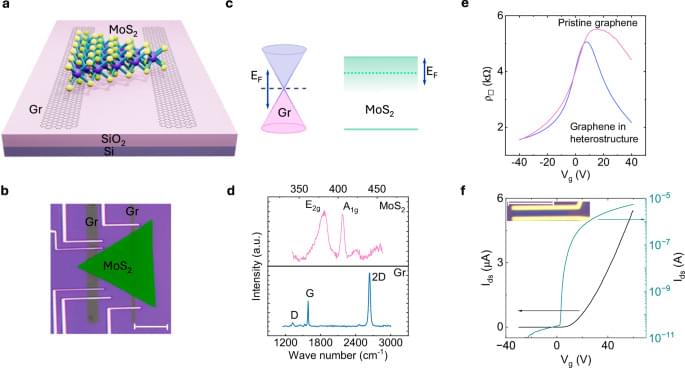
All-2D CVD-grown semiconductor field-effect transistors with van der Waals graphene contacts
Hoque, M.A., George, A., Ramachandra, V. et al. All-2D CVD-grown semiconductor field-effect transistors with van der Waals graphene contacts. npj 2D Mater Appl 8, 55 (2024). https://doi.org/10.1038/s41699-024-00489-2

US achieves superconductor breakthrough, can benefit quantum computing
A team of scientists in the United States has achieved a notable milestone in the domain of superconductors. This progress may have considerable consequences for the future of quantum computing.
The research details the development of a novel superconductor material that has the potential to transform quantum computing and potentially function as a “topological superconductor.”
A topological superconductor is a special kind of material that exhibits superconductivity (zero electrical resistance) and also has unique properties related to its shape or topology.

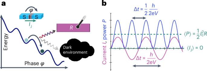
Bolometric detection of Josephson radiation
An on-chip nano-bolometer integrated with a Josephson junction quantitatively measures the Josephson radiation up to about 100 GHz frequency. This wide-band, thermal detection scheme of microwave photons provides a sensitive detector of Josephson dynamics beyond the standard conductance measurements.

Neuralink’s second patient is using his brain implant to design 3D objects. Here’s how it works
Neuralink says it has successfully implanted another brain chip in a human patient.
According to a study update shared by the company, the patient, identified by his first name, Alex, has been improving his ability to play video games and has started learning how to use design software to create 3D objects.
The company said the procedure “went well,” and Alex’s recovery “has been smooth.”
What is IBM doing in the race towards quantum computing?
Quantum computing is in all likelihood the 21st century’s great computer revolution. What is IBM doing to make the quantum dream a reality?

How close are we to mind uploading? The science and challenges of whole brain emulation
Have you ever wondered what it would be like to upload your mind to a computer? To have a digital copy of your personality, memories, and skills that could live on after your biological death? This is the idea behind whole brain emulation, a hypothetical process of scanning a brain and creating a software version of it that can run on any compatible hardware. In this video, we will explore the science and challenges of whole brain emulation, the ethical and social implications of creating digital minds, and the potential benefits and risks of this technology for humanity. Join us as we dive into the fascinating world of whole-brain emulation!
#wholebrainemulation.
#minduploading.
#digitalimmortality.
#artificialintelligence.
#neuroscience.
#braincomputerinterface.
#substrateindependentminds.
#transhumanism.
#futurism.
#mindcloning

Brain prosthesis passes live tissue test
The world’s first brain prosthesis has passed the first stages of live testing.
The microchip, designed to model a part of the brain called the hippocampus, has been used successfully to replace a neural circuit in slices of rat brain tissue kept alive in a dish. The prosthesis will soon be ready for testing in animals.
The device could ultimately be used to replace damaged brain tissue which may have been destroyed in an accident, during a stroke, or by neurodegenerative conditions such as Alzheimer’s disease. It is the first attempt to replace central brain regions dealing with cognitive functions such as learning or speech.

New Materials Identified for Protecting Astronauts from Mars Radiation
“This breakthrough enhances astronaut safety and makes long-term Mars missions a more realistic possibility,” said Dr. Dimitra Atri.
How will future Mars astronauts shield themselves from harmful space radiation? This is what a recent study published in The European Physical Journal Plus hopes to address as a pair of international researchers investigated what materials could be suited for providing the necessary shielding against solar and cosmic rays that could harm future Mars astronauts. This study holds the potential to help scientists and engineers better understand the mitigation measures that need to be taken to protect astronauts during long-term space missions.
For the study, the researchers used computer simulations to create Mars-like conditions, whose surface temperatures and pressures are much smaller than Earth’s, along with Mars completely lacking a protective magnetic field that provides our planet with protection from space radiation. Through this, the researchers tested a variety of materials to ascertain their effectiveness in shielding astronauts from space radiation.
In the end, they found that synthetic fibers, rubber, and plastics demonstrated the best performance of providing shielding. Additionally, the team found that Martian regolith (commonly called Martian “soil”) and aluminum combined with other materials could also be effective as a shielding agent, as well.