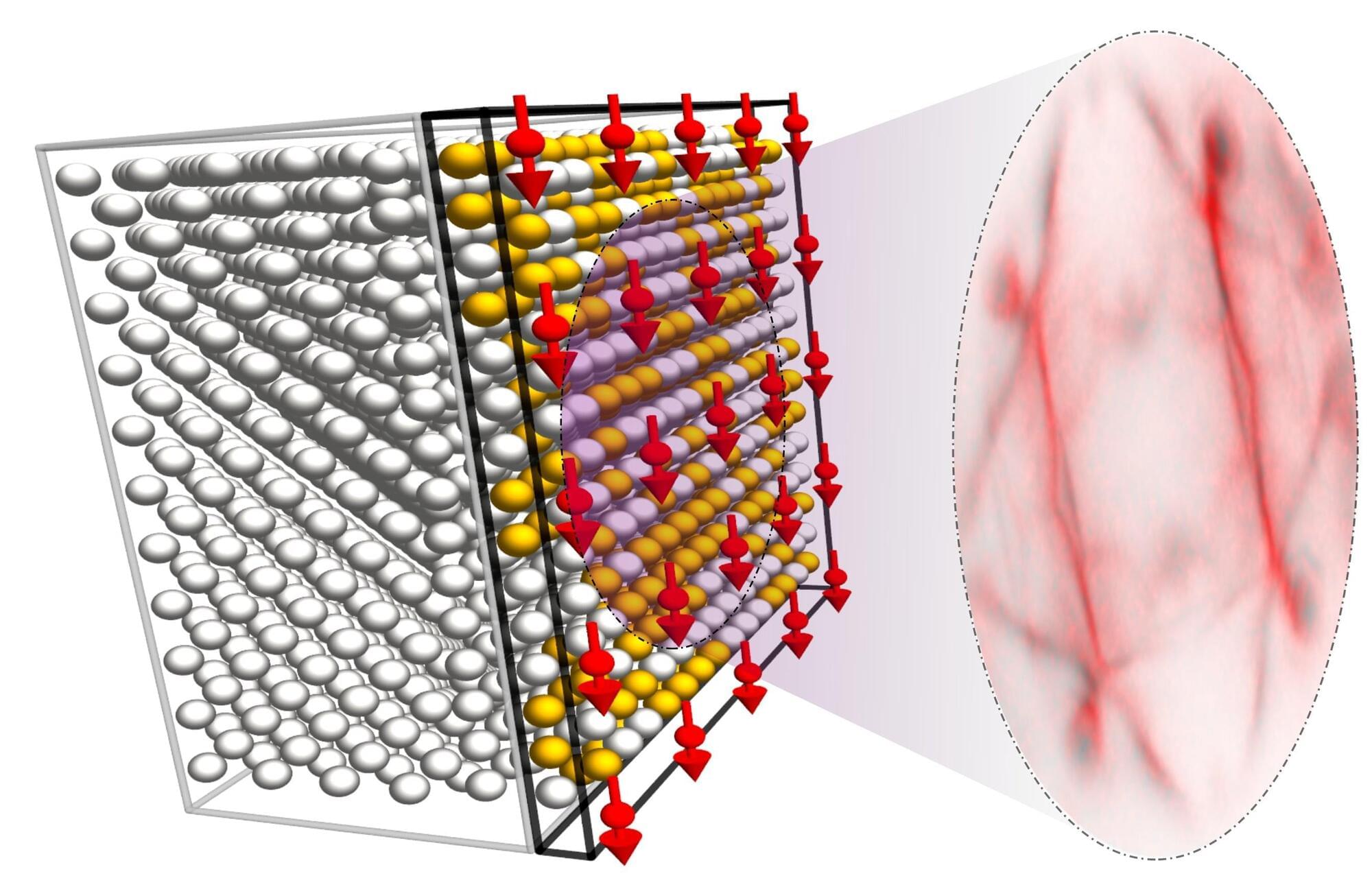
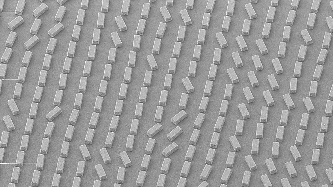
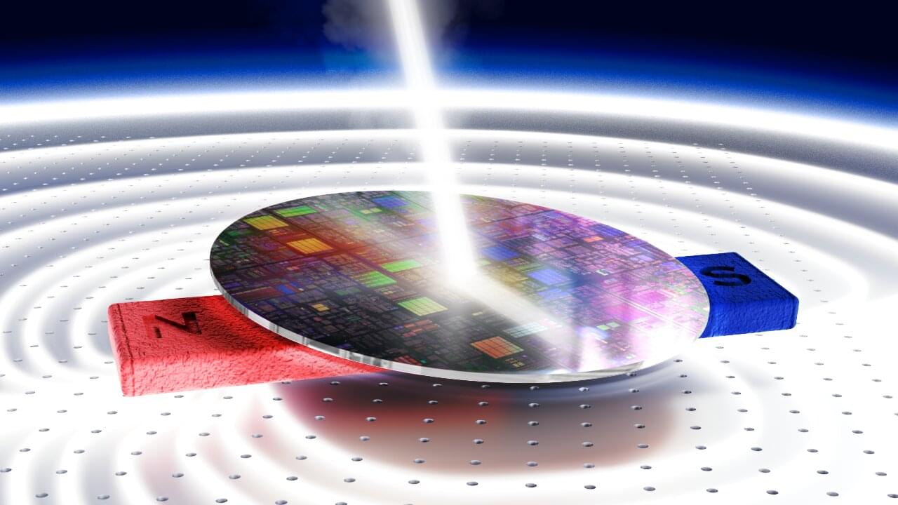
Toggle light / dark theme

Dynamic visualizations expose how domain walls shift in ferroelectrics

As demand for energy-intensive computing grows, researchers at the Department of Energy’s Oak Ridge National Laboratory have developed a new technique that lets scientists see—in unprecedented detail—how interfaces move in promising materials for computing and other applications. The method, now available to users at the Center for Nanophase Materials Sciences at ORNL, could help design dramatically more energy-efficient technologies.

The research is published in the journal Small Methods.

Data centers today consume as much energy as small cities, and that usage is skyrocketing. To counter the trend, scientists are studying such as ferroelectrics that could store and process information far more efficiently than silicon, which is traditionally used. But realizing the potential depends on understanding the processes occurring at dimensions thousands of times smaller than a —specifically, at the ferroelectric material’s , which are the boundaries between areas of the material that exhibit different magnetic or electric properties.

Gravity could be the definitive clue that the universe is a computer

Modern ideas about reality sometimes sound like a wild story. The notion that everything around us might be bits and bytes is easy to brush aside, yet it continues to intrigue many curious minds.

This perspective has led some researchers to wonder if physical forces might be signals of an underlying information system.

According to physicist Melvin M. Vopson of the University of Portsmouth, certain features of gravity may hint at information contained in a universal computational code.

Novel material design enables pure-red perovskite LEDs with record-breaking performance

A team from the University of Science and Technology of China (USTC) of the Chinese Academy of Sciences (CAS) has resolved a critical challenge in pure-red perovskite light-emitting diodes (PeLEDs) by identifying and addressing the root cause of efficiency loss at high brightness.

Published in Nature, their study introduces a novel material design that enables record-breaking device performance, achieving a peak external quantum efficiency (EQE) of 24.2% and a maximum luminance of 24,600 cd m-2 —the brightest pure-red PeLED reported to date.

Pure-red PeLEDs, crucial for vivid displays and lighting, have long faced a trade-off between efficiency and brightness. While 3D mixed-halide perovskites like CsPbI3-x Brx offer excellent charge transport, their efficiency plummets under high current due to unresolved carrier leakage.

Topological polycrystal: A new approach to configurable, multiband topological photonic circuitry

Molding the flow of light—whether confined to localized regions or propagating in free space—remains crucial for modern integrated photonics. The advancement of the multi-channel, programmable optical waveguide and coupler arrays has enabled us to develop photonic integrated circuits (PICs) as a viable alternative to electronic ones, overcoming limitations in processing speed, bandwidth, and efficiency across the optical-to-microwave spectrum.

However, as on-chip complexity grows, we face significant challenges regarding long-term stability and fabrication-induced defects, making operational reliability critical for practical applications.

The increasing demand for high-capacity information processing drives our need for more complex PICs with additional channels. In this context, topological photonics offers promising solutions due to its inherent robustness against defects.

/* */