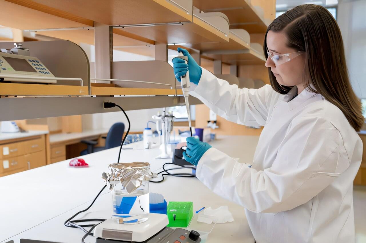
Additive manufacturing, or 3D printing, is normally a one-way street. In a digital light processing (DLP) printer, a structured pattern is projected onto a layer of liquid resin, which cures and solidifies. This builds an object up, layer-by-layer. But if the print isn’t exactly right, there’s no easy way to fix it after the fact: it usually ends up in the trash.
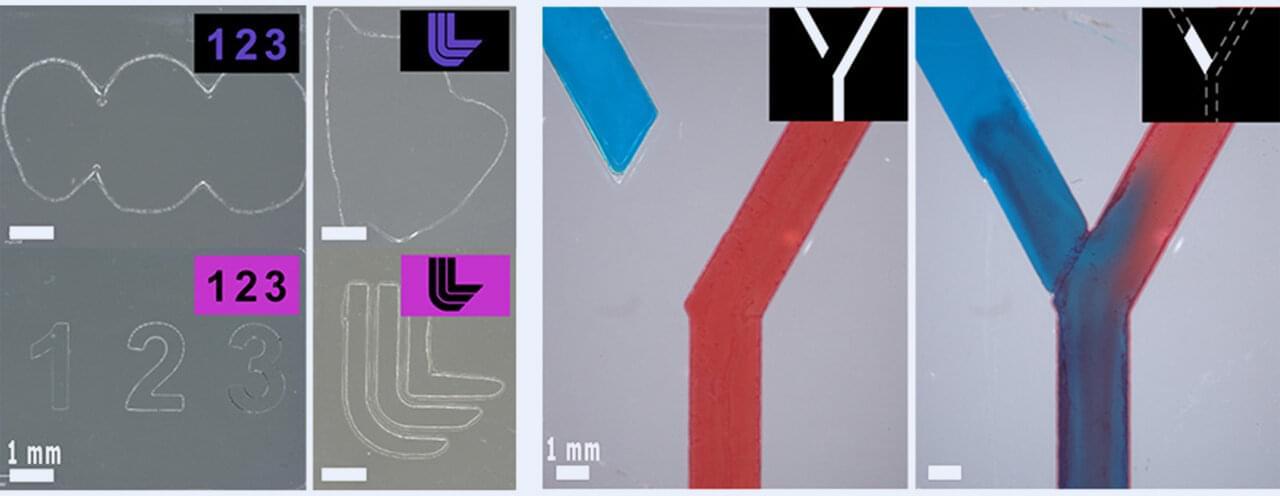
In a new study, published in Advanced Materials Technologies, researchers at Lawrence Livermore National Laboratory (LLNL) developed a hybrid additive and subtractive manufacturing system with a unique resin that enhances traditional 3D printing by introducing dual-wavelength behavior. Under blue light, the resin cures and hardens. Under ultraviolet light, it degrades back into a liquid. The hybrid printing system enables corrective manufacturing, provides improved print resolution and allows for upcycling and recycling of parts.
“Imagine if a company needed a part to fit a certain machine but it’s a prototype and they’re not quite sure what they want,” said LLNL scientist and author Benjamin Alameda. “They could theoretically print with our resin. And if there were defects or something they wanted to change about it, they don’t have to print a whole new part. They could just shine another wavelength on it and modify the existing part. That’s useful and less wasteful.”