Study finds Claude in Arabic uses more ‘polite phrasing’ and showed ‘greater warmth’ than other language models


Artificial intelligence (AI) models are now used daily by many people worldwide, both for professional and personal purposes. Over the past decades, scientists specialized in various disciplines have also started using these models to conduct research or simplify their experimental practices.
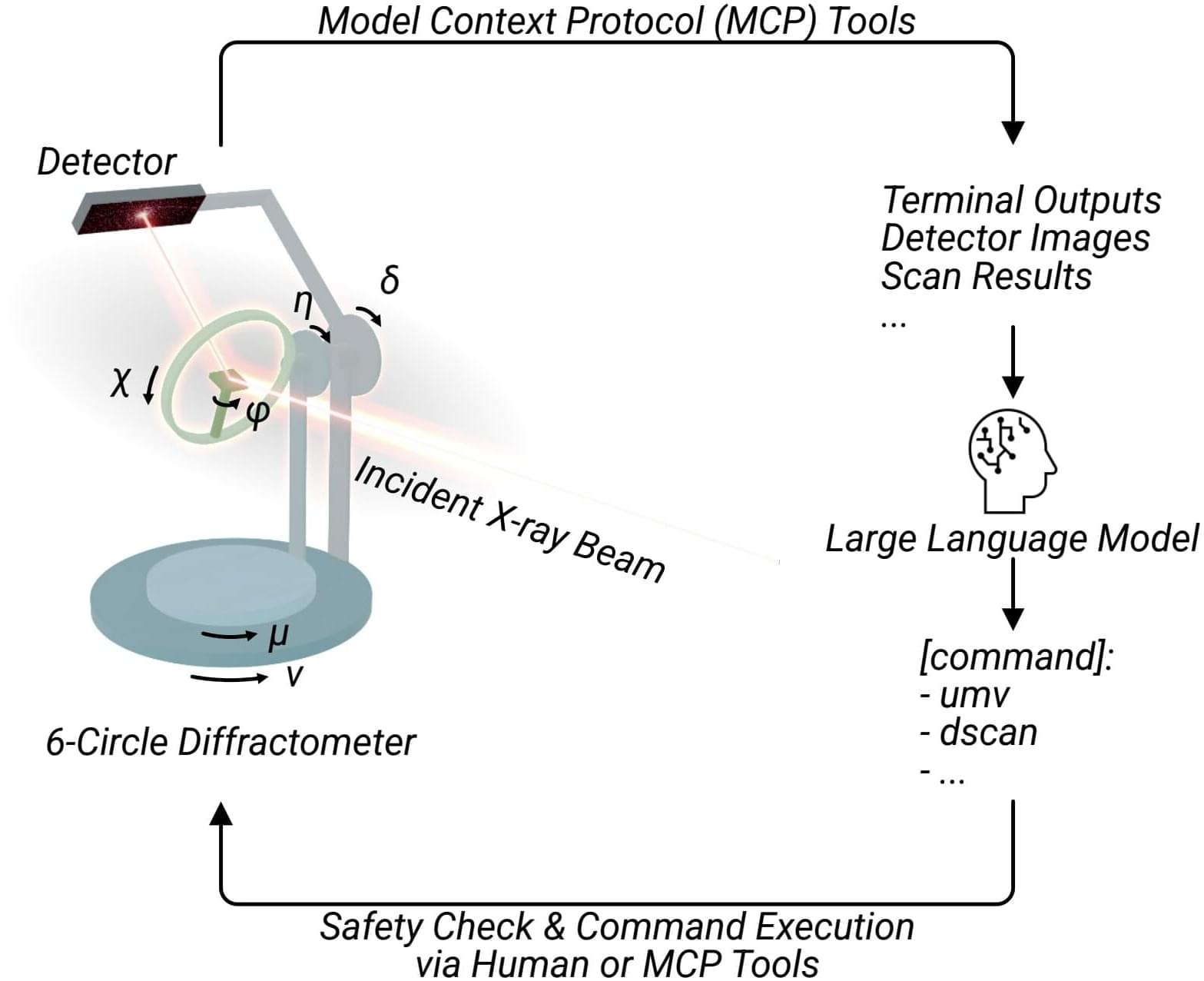
Researchers at Stanford University and SLAC National Accelerator Laboratory recently explored the possibility of using an AI-powered agent to prepare a synchrotron-based X-ray experiment. Synchrotrons are large research facilities at which electrons are accelerated to produce very bright X-rays, which can then be used to study the atomic structure of materials, molecules and biological samples.
In a paper published in Nature Machine Intelligence, the team at Stanford and SLAC proposed using an AI-based agent to prepare a real synchrotron X-ray experiment. They showed that this agent could autonomously plan actions, interpret observations and generate instrument-control commands to complete sample alignment.

No wires. No actuators. Shine light on the metal surface, and it rises like a button. KAIST researchers have developed a metal structure that changes shape using light, without any light-absorbing coating. This technology could open new possibilities for tactile interfaces with physical pop-up buttons, shape displays, next-generation wearable devices and soft robots.
A research team led by Professor Il-Kwon Oh from the Department of Mechanical Engineering has developed a technology that transforms a flat NiTi shape-memory alloy (SMA) sheet into a “photothermally driven meta-morphing structure” that rises from a flat surface into a three-dimensional form when exposed to light, using only a single UV laser process.
The results are published in the journal Advanced Science.


The industry spent the initial months after Anthropic’s April 7 Mythos reveal focused on volume. How many new CVEs would Mythos add to an already overloaded pipeline? How quickly would the flood of AI-driven discovery overwhelm triage capabilities? How long would it take adversaries to weaponize Mythos findings at scale? Those questions were and remain valid. Yet they all stop short of addressing the single metric that determines whether any of those vulnerabilities actually lead to a breach: the exposure window.
The exposure window — the gap between the moment a vulnerability becomes exploitable and the moment your team fixes it — is the time an attacker has to do actual damage. That window is currently open far too wide. In 2025, the average eCrime breakout time dropped to 29 minutes. Even PCI DSS — the strictest compliance framework in the industry — allows 30 days to remediate a critical vulnerability. That’s a 1,000-to-1 gap between how fast attackers move and how fast organizations are expected to respond. And the stick propping this exposure window open? Mobilization — the ownership, remediation, and organizational complexity that lowers response times and raises risk.
In this article, I’ll walk through why the exposure window is now the metric that matters most, what keeps it open, and how AI-driven discovery is forcing proactive security teams to adopt the speed-based metrics that SOC teams have used for years.


TradingKey — According to a report from The Information citing two people familiar with the matter, Google (GOOGL) is developing a new server chip capable of directly embedding the underlying architecture of the Gemini large model into the chip hardware to significantly enhance the operational efficiency of AI services for users. Internally codenamed “Frozen v2,” this AI inference chip directly addresses Google’s current severe shortage of AI computing power. Sources revealed that the computing capacity gap has triggered internal resource conflicts and even forced Google Cloud to reject numerous orders from external customers. The research and development team estimates that once the chip is officially deployed, the number of tokens processed per unit of power consumption will be 6 to 10 times that of the latest generation of Google’s existing self-developed AI chips.

Gelonghui, July 13 | According to Science and Technology Daily, the surge in AI technology has driven strong demand for advanced chips, yet global chip supply remains constrained by the technology and production capacity of only a few companies. In a recent report, Forbes.com noted that as emerging technologies continue to rise, the global approach to manufacturing cutting-edge chips is expected to undergo a major transformation by 2030. Although extreme ultraviolet (EUV) lithography is currently dominant, it is not the only method for ‘drawing’ microscopic transistors onto silicon wafers. A new generation of forward-looking lithography technologies is poised to emerge, potentially replacing EUV lithography and reshaping how advanced chips are manufactured. Atomic lithography abandons ‘light’ and instead