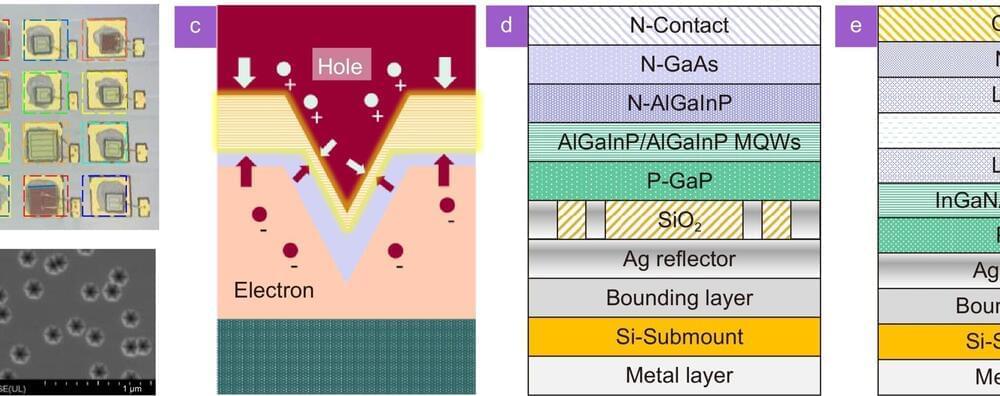
Under the limitation of current density, micro-LED is difficult to achieve watts level optical power, which is not suitable for long-distance and underwater optical communication that requires high-power optical transmitter devices. Therefore, how to improve the communication performance of conventional-size LED is also a key issue at present.
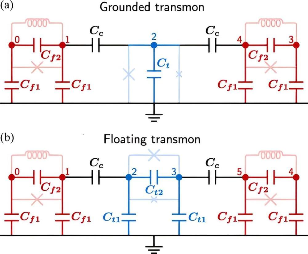
The authors of an article published in Opto-Electronic Science studied a wavelength division multiplexing visible light communication system based on multi-color LED. The system uses a Si substrate GaN-based LED with a 3D structured quantum well. In the active layer of this LED, there is a three-dimensional structure (“V” shaped pit, or V-pit) with a hexagonal profile, opening towards the P-type GaN layer.
With the large-scale commercial use of 5G, global academia and industry have started research on the next-generation mobile communication technology (6G).
However, the existing RF spectrum resources are seriously depleted to meet the spectrum demand of 6G for ultra-high speed and ultra-large capacity. This severe challenge stimulates researchers to focus on higher frequency bands such as terahertz, infrared and visible light. Among them, visible light communication utilizes the ultra-wide spectrum from 400THz to 800THz, which has the merits of no licensing, high secrecy, environmental-friendly, and no electromagnetic radiation.
At the same time, with the help of commercially available LED technology, visible light communication systems can be integrated with lighting systems. However, limited by the electro-optic response performance of LED devices, the actual available bandwidth of the system is very small compared with the frequency band of visible light.