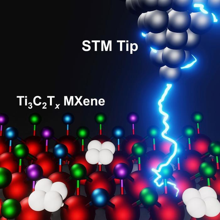
Toggle light / dark theme

LeviPrint is a system that uses acoustic manipulation for assembling objects without physical contact. It generates acoustic fields that trap small particles, glue droplets and elongated stick-like elements that can be manipulated and reoriented as they are levitated. It is a fully functional system for manufacturing 3D structures using contactless manipulation.

It was developed by researchers from the UPNA/NUP-Public University of Navarre Asier Marzo and Iñigo Ezcurdia, who together with Rafael Morales (Ultraleap Ltd, UK) and Marco Andrade (University of São Paulo, Brazil) are authors of the paper “LeviPrint: Contactless Fabrication using Full Acoustic Trapping of Elongated Parts.”

This research is due to be presented in August in Vancouver (Canada) at SIGGRAPH, a conference on and where companies such as Nvidia, Disney Research and Facebook Reality Labs present their work.

To solve a long-standing puzzle about how long a neutron can “live” outside an atomic nucleus, physicists entertained a wild but testable theory positing the existence of a right-handed version of our left-handed universe. They designed a mind-bending experiment at the Department of Energy’s Oak Ridge National Laboratory to try to detect a particle that has been speculated but not spotted. If found, the theorized “mirror neutron”—a dark-matter twin to the neutron—could explain a discrepancy between answers from two types of neutron lifetime experiments and provide the first observation of dark matter.

“Dark matter remains one of the most important and puzzling questions in science—clear evidence we don’t understand all matter in nature,” said ORNL’s Leah Broussard, who led the study published in Physical Review Letters.

Neutrons and protons make up an atom’s nucleus. However, they also can exist outside nuclei. Last year, using the Los Alamos Neutron Science Center, co-author Frank Gonzalez, now at ORNL, led the most precise measurement ever of how long free neutrons live before they decay, or turn into protons, electrons and anti-neutrinos. The answer—877.8 seconds, give or take 0.3 seconds, or a little under 15 minutes—hinted at a crack in the Standard Model of particle physics. That model describes the behavior of subatomic particles, such as the three quarks that make up a neutron. The flipping of quarks initiates neutron decay into protons.

The ever-increasing production and use of plastics over the last half century has created a huge environmental problem for the world. Currently, most of the 4.9 billion tonnes of plastics ever produced will end up in landfills or the natural environment, and this number is expected to increase to around 12 billion tonnes by 2050.

In collaboration with colleagues at universities and institutions in the UK, China and the Kingdom of Saudi Arabia, researchers in the Edwards/ Xiao group at Oxford’s Department of Chemistry have developed a method of converting plastic waste into hydrogen gas which can be used as a clean fuel, and high-value solid carbon. This was achieved with a new type of catalysis developed by the group which uses microwaves to activate catalyst particles to effectively ‘strip’ hydrogen from polymers.

The findings, published in Nature Catalysis, detail how the researchers mixed mechanically-pulverised plastic particles with a microwave-susceptor catalyst of iron oxide and aluminium oxide. The mixture was subjected to microwave treatment and yielded a large volume of hydrogen gas and a residue of carbonaceous materials, the bulk of which were identified as carbon nanotubes.

Operators of the ALICE detector have observed the first direct evidence of the “dead cone effect,” allowing them to assess the mass of the elusive charm quark.


The ALICE collaboration at the Large Hadron Collider (LHC) in Geneva, Switzerland, recently made the first observation of an important aspect of particle physics called the “dead cone effect.”

The effect is a fundamental element of the strong nuclear force — one of the four fundamental forces of nature — responsible for binding quarks and gluons. These are the fundamental particles that comprise hadrons, such as protons and neutrons, that in turn make up all atomic nuclei, which are never seen on their own under normal circumstances, only at the kind of high energy levels generated at the LHC.

“We made a direct observation of an effect in the theory of the strong force called the dead-cone effect,” experimental high energy physicist at CERN, Nima Zardoshti, tells Popular Mechanics. “This is a part of the theory that had been predicted for a while but had not been directly observed until now.”

Whether or not a solid can emit light, for instance as a light-emitting diode (LED), depends on the energy levels of the electrons in its crystalline lattice. An international team of researchers led by University of Oldenburg physicists Dr. Hangyong Shan and Prof. Dr. Christian Schneider has succeeded in manipulating the energy-levels in an ultra-thin sample of the semiconductor tungsten diselenide in such a way that this material, which normally has a low luminescence yield, began to glow. The team has now published an article on its research in the science journal Nature Communications.

According to the researchers, their findings constitute a first step towards controlling the properties of matter through light fields. “The idea has been discussed for years, but had not yet been convincingly implemented,” said Schneider. The light effect could be used to optimize the optical properties of semiconductors and thus contribute to the development of innovative LEDs, , optical components and other applications. In particular the optical properties of organic semiconductors—plastics with semiconducting properties that are used in flexible displays and solar cells or as sensors in textiles—could be enhanced in this way.

Tungsten diselenide belongs to an unusual class of semiconductors consisting of a and one of the three elements sulfur, selenium or tellurium. For their experiments the researchers used a sample that consisted of a single crystalline layer of and selenium atoms with a sandwich-like structure. In physics, such materials, which are only a few atoms thick, are also known as two-dimensional (2D) materials. They often have unusual properties because the they contain behave in a completely different manner to those in thicker solids and are sometimes referred to as “quantum materials.”

Researchers at the University of New South Wales and a startup company, Silicon Quantum Computing, published results of their quantum dot experiments. The circuits use up to 10 carbon-based quantum dots on a silicon substrate. Metal gates control the flow of electrons. The paper appears in Nature and you can download the full paper from there.

What’s new about this is that the dots are precisely arranged to simulate an organic compound, polyacetylene. This allowed researchers to model the actual molecule. Simulating molecules is important in the study of exotic matter phases, such as superconductivity. The interaction of particles inside, for example, a crystalline structure is difficult to simulate using conventional methods. By building a model using quantum techniques on the same scale and with the same topology as the molecule in question, simulation is simplified.

The SSH (Su-Schreffer-Heeger) model describes a single electron moving along a one-dimensional lattice with staggered tunnel couplings. At least, that’s what the paper says and we have to believe it. Creating such a model for simple systems has been feasible, but for a “many body” problem, conventional computing just isn’t up to the task. Currently, the 10 dot model is right at the limit of what a conventional computer can simulate reasonably. The team plans to build a 20 dot circuit that would allow for unique simulations not feasible with classic computing tech.

Transistors are the building blocks of modern electronics, used in everything from televisions to laptops. As transistors have gotten smaller and more compact, so have electronics, which is why your cell phone is a super powerful computer that fits in the palm of your hand.

But there’s a scaling problem: Transistors are now so small that they are difficult to turn off. A key device element is the channel that charge carriers (such as electrons) travel across between electrodes. If that channel gets too short, allow electrons to effectively jump from one side to another even when they shouldn’t.

One way to get past this sizing roadblock is to use layers of 2D materials—which are only a single atom thick—as the channel. Atomically thin channels can help enable even smaller transistors by making it harder for the electrons to jump between electrodes. One well-known example of a 2D material is graphene, whose discoverers won the Nobel Prize in Physics in 2010. But there are other 2D materials, and many believe they are the future of transistors, with the promise of scaling channel thickness down from its current 3D limit of a few nanometers (nm, billionths of a meter) to less than a single nanometer thickness.