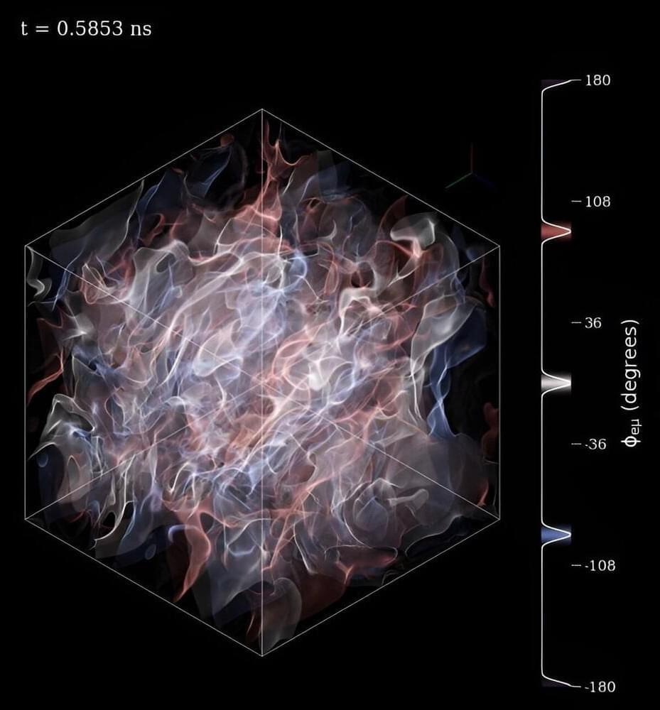
Toggle light / dark theme

Operators of the ALICE detector have observed the first direct evidence of the “dead cone effect,” allowing them to assess the mass of the elusive charm quark.


The ALICE collaboration at the Large Hadron Collider (LHC) in Geneva, Switzerland, recently made the first observation of an important aspect of particle physics called the “dead cone effect.”

The effect is a fundamental element of the strong nuclear force — one of the four fundamental forces of nature — responsible for binding quarks and gluons. These are the fundamental particles that comprise hadrons, such as protons and neutrons, that in turn make up all atomic nuclei, which are never seen on their own under normal circumstances, only at the kind of high energy levels generated at the LHC.

“We made a direct observation of an effect in the theory of the strong force called the dead-cone effect,” experimental high energy physicist at CERN, Nima Zardoshti, tells Popular Mechanics. “This is a part of the theory that had been predicted for a while but had not been directly observed until now.”

Whether or not a solid can emit light, for instance as a light-emitting diode (LED), depends on the energy levels of the electrons in its crystalline lattice. An international team of researchers led by University of Oldenburg physicists Dr. Hangyong Shan and Prof. Dr. Christian Schneider has succeeded in manipulating the energy-levels in an ultra-thin sample of the semiconductor tungsten diselenide in such a way that this material, which normally has a low luminescence yield, began to glow. The team has now published an article on its research in the science journal Nature Communications.

According to the researchers, their findings constitute a first step towards controlling the properties of matter through light fields. “The idea has been discussed for years, but had not yet been convincingly implemented,” said Schneider. The light effect could be used to optimize the optical properties of semiconductors and thus contribute to the development of innovative LEDs, , optical components and other applications. In particular the optical properties of organic semiconductors—plastics with semiconducting properties that are used in flexible displays and solar cells or as sensors in textiles—could be enhanced in this way.

Tungsten diselenide belongs to an unusual class of semiconductors consisting of a and one of the three elements sulfur, selenium or tellurium. For their experiments the researchers used a sample that consisted of a single crystalline layer of and selenium atoms with a sandwich-like structure. In physics, such materials, which are only a few atoms thick, are also known as two-dimensional (2D) materials. They often have unusual properties because the they contain behave in a completely different manner to those in thicker solids and are sometimes referred to as “quantum materials.”

Researchers at the University of New South Wales and a startup company, Silicon Quantum Computing, published results of their quantum dot experiments. The circuits use up to 10 carbon-based quantum dots on a silicon substrate. Metal gates control the flow of electrons. The paper appears in Nature and you can download the full paper from there.

What’s new about this is that the dots are precisely arranged to simulate an organic compound, polyacetylene. This allowed researchers to model the actual molecule. Simulating molecules is important in the study of exotic matter phases, such as superconductivity. The interaction of particles inside, for example, a crystalline structure is difficult to simulate using conventional methods. By building a model using quantum techniques on the same scale and with the same topology as the molecule in question, simulation is simplified.

The SSH (Su-Schreffer-Heeger) model describes a single electron moving along a one-dimensional lattice with staggered tunnel couplings. At least, that’s what the paper says and we have to believe it. Creating such a model for simple systems has been feasible, but for a “many body” problem, conventional computing just isn’t up to the task. Currently, the 10 dot model is right at the limit of what a conventional computer can simulate reasonably. The team plans to build a 20 dot circuit that would allow for unique simulations not feasible with classic computing tech.

Transistors are the building blocks of modern electronics, used in everything from televisions to laptops. As transistors have gotten smaller and more compact, so have electronics, which is why your cell phone is a super powerful computer that fits in the palm of your hand.

But there’s a scaling problem: Transistors are now so small that they are difficult to turn off. A key device element is the channel that charge carriers (such as electrons) travel across between electrodes. If that channel gets too short, allow electrons to effectively jump from one side to another even when they shouldn’t.

One way to get past this sizing roadblock is to use layers of 2D materials—which are only a single atom thick—as the channel. Atomically thin channels can help enable even smaller transistors by making it harder for the electrons to jump between electrodes. One well-known example of a 2D material is graphene, whose discoverers won the Nobel Prize in Physics in 2010. But there are other 2D materials, and many believe they are the future of transistors, with the promise of scaling channel thickness down from its current 3D limit of a few nanometers (nm, billionths of a meter) to less than a single nanometer thickness.

Researchers in Switzerland and Italy have developed a new method for generating currents of spin-polarized electrons without the need for large external magnetic fields. This could enable the development of devices that are compatible with superconducting electronic components, paving the way for the next generation of highly efficient electronics.

Emerging in the 1980s, “spintronics” is dedicated to creating practical devices that exploit electron spin. Semiconductor-based spintronics systems have garnered particular interest because semiconductors can be integrated within modern-day electronics with the aim of improving the efficiency and storage capacity of devices. But to make useful spintronics devices, researchers must control and detect the spin state of electrons with a high level of accuracy.

One way of controlling electron spin current is a “spin valve”, which usually consists of a non-magnetic material sandwiched between ferromagnetic materials. Electrons in one spin state (say up) can propagate through the device, while spin-down electrons are reflected or scattered away. The result is a “spin polarized current” in which all electrons are either spin-up or all spin-down) – at least in principle.

Researchers in the US, Poland and Korea have observed photon avalanching – a chain-reaction-like process in which the absorption of a single photon triggers the emission of many – in tiny crystals just 25–30 nm in diameter. This highly nonlinear phenomenon had previously only been seen in bulk materials, and team leader James Schuck says that replicating it in nanoparticles could lead to “revolutionary new applications” in imaging, sensing and light detection (Nature 589 230).

Photon avalanching involves a process known as upconversion, whereby the energy of the emitted photons is higher than the energy of the photons that triggered the avalanche. Materials based on lanthanides (chemical elements with atomic numbers between 57 and 71) can support this process in part because their internal atomic structure enables them to store energy for long periods of time. Even so, achieving photon avalanching in lanthanide systems is difficult because high concentrations of lanthanide ions are needed to keep the avalanche going, and the relatively large volume of material required has previously restricted applications.

In the latest work, Schuck and colleagues at Columbia University, together with collaborators at Lawrence Berkeley National Laboratory, the Polish Academy of Sciences and Sungkyunkwan University, observed photon avalanching in lanthanide nanocrystals after exciting them with a laser at near-infrared wavelengths of either 1,064 or 1450 nm. The crystals are based on sodium yttrium fluoride in which 8% of the yttrium ions have been replaced with thulium. This doping fraction is much higher than the 0.2–1% typically found in previous work on photon avalanching.

Two research groups demonstrate quantum algorithms using neutral atoms as qubits. Tim Wogan reports.

The first quantum processors that use neutral atoms as qubits have been produced independently by two US-based groups. The result offers the possibility of building quantum computers that could be easier to scale up than current devices.

Two technologies have dominated quantum computing so far, but they are not without issues. Superconducting qubits must be constructed individually, making it nearly impossible to fabricate identical copies, so the probability of the output being correct is reduced – causing what is known as “gate fidelity”. Moreover, each qubit must be cooled close to absolute zero. Trapped ions, on the other hand, have the advantage that each ion is guaranteed to be indistinguishable by the laws of quantum mechanics. But while ions in a vacuum are relatively easy to isolate from thermal noise, they are strongly interacting and so require electric fields to move them around.

Pedram Roushan, from Google’s Quantum AI team in California, describes this elusive form of matter – and how it could be simulated on the company’s Sycamore quantum processor.

With their enchanting beauty, crystalline solids have captivated us for centuries. Crystals, which range from snowflakes to diamonds, are made up of atoms or molecules that are regularly arranged in space. They have provided foundational insights that led to the development of the quantum theory of solids. Crystals have also helped develop a framework for understanding other spatially ordered phases, such as superconductors, liquid crystals and ferromagnets.

Periodic oscillations are another ubiquitous phenomenon. They appear at all scales, ranging from atomic oscillations to orbiting planets. For many years, we used them to mark the passage of time, and they even made us ponder the possibility of perpetual motion. What is common between these periodic patterns – either in space or time – is that they lead to systems with reduced symmetries. Without periodicity, any position in space, or any instance of time, is indistinguishable from any other. Periodicity breaks the translational symmetry of space or time.