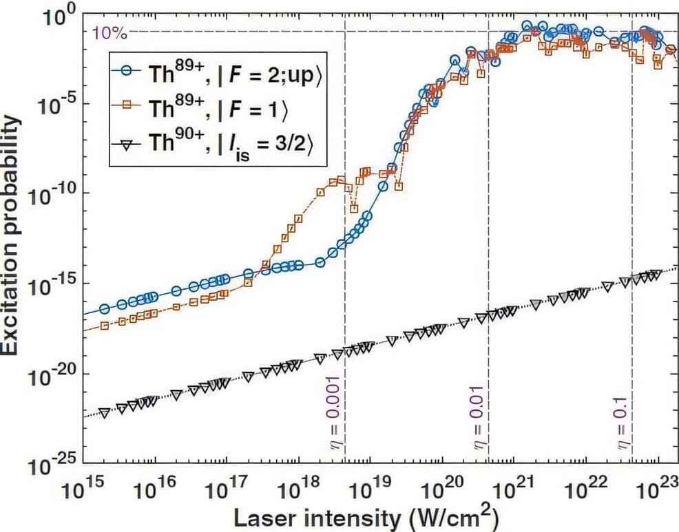
Why are there atomic clocks but no nuclear clocks? After all, an atom’s nucleus is typically surrounded by many electrons, so in principle it should be less susceptible to outside noise (in the form of light). A nucleus, for high-atomic number atoms, contains more particles than does the element’s electrons. It holds nearly the entire mass of the atom while taking up only about 1/100,000th of the atom’s space. While the first atomic clock was invented in 1949, no nuclear clock has yet been feasible.
Category: particle physics – Page 257
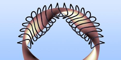
A New Twist on Stellarator Design
Breaking the problem into pieces makes it easier to design a fusion reactor’s coils for optimum energy confinement.
In magnetic-confinement fusion, different reactor designs pose different trade-offs. Stellarators use external magnetic fields to confine plasma in the shape of a twisted donut. Such fields are relatively easy to maintain in a steady state, but optimizing their geometry to minimize energy loss is much more difficult. Tokamaks, in contrast, confine plasma in an axisymmetric geometry using magnetic fields partially generated via currents induced in the plasma. This geometry provides near-perfect confinement at the expense of stability and operational simplicity. José Luis Velasco of Spain’s Center for Energy, Environmental and Technological Research (CIEMAT) and his colleagues now present a new family of stellarator magnetic-field configurations that benefit from tokamak-like energy confinement [1].
Magnetic fusion designs achieve confinement using nested magnetic-flux surfaces. Ideally, each charged particle remains tied to a given surface contour and the plasma as a whole exhibits near-zero radial drift. Such a condition results in perfect confinement, aside from losses due to collisions among particles on the same contour. Tokamaks inherently avoid radial drift, but to achieve the same level of confinement in a stellarator means imposing constraints on each magnetic surface’s topology, sometimes requiring infeasible coil designs.
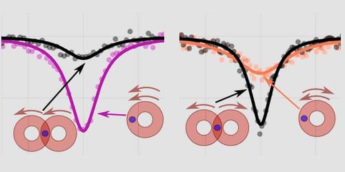
Probing the Rotational Doppler Effect with a Single Ion
A light beam with orbital angular momentum can produce the rotational analog of the Doppler effect on an ion.
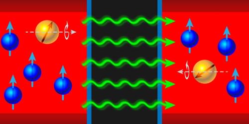
A vortex light beam is one whose wave fronts rotate like a corkscrew, endowing the beam with orbital angular momentum. An atom subjected to this beam experiences the usual kick in the direction of the beam’s propagation but also a weaker, sideways kick from the beam’s orbital angular momentum. The Doppler effect causes a moving atom to absorb light at wavelengths that are shifted with respect to those of a stationary atom. Consequently, the sideways kick from a vortex beam can produce what is called a rotational Doppler effect (RDE) in an atom. Nicolás Nuñez Barreto of the University of Buenos Aires in Argentina and his collaborators have now characterized the RDE produced by infrared (IR) vortex beams on a single trapped calcium ion [1].
The researchers used IR lasers to drive a particular transition between electronic levels of the ion in a magnetic field. Two additional IR lasers created two identical copropagating vortex beams whose wavelengths could be adjusted. Thanks to the copropagation and the nature of the transition, the linear Doppler effects of the two beams canceled out. Only when the ion received different sideways kicks resulting from the beams’ unequal angular momenta did it absorb photons, revealing the presence and strength of the RDE.
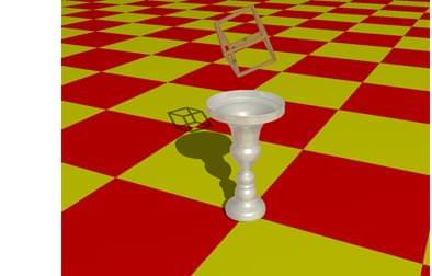
Quantum-tunneling deep neural network for optical illusion recognition
The discovery of the quantum tunneling (QT) effect—the transmission of particles through a high potential barrier—was one of the most impressive achievements of quantum mechanics made in the 1920s. Responding to the contemporary challenges, I introduce a deep neural network (DNN) architecture that processes information using the effect of QT. I demonstrate the ability of QT-DNN to recognize optical illusions like a human. Tasking QT-DNN to simulate human perception of the Necker cube and Rubin’s vase, I provide arguments in favor of the superiority of QT-based activation functions over the activation functions optimized for modern applications in machine vision, also showing that, at the fundamental level, QT-DNN is closely related to biology-inspired DNNs and models based on the principles of quantum information processing.
Searching for Axions in Polarized Gas
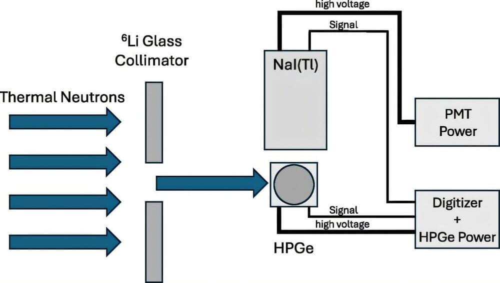
The standard model of fundamental particles and interactions has now been in place for about a half-century. It has successfully passed experimental test after experimental test at particle accelerators. However, many of the model’s features are poorly understood, and it is now clear that standard-model particles only compose about 5% of the observed energy density of the Universe. This situation naturally encourages researchers to look for new particles and interactions that fall outside this model. One way to perform this search is to prepare a gas of polarized atoms and to look for changes in this polarization that might come from new physics. Haowen Su from the University of Science and Technology of China and colleagues have used two separated samples of polarized xenon gas to probe spin-dependent interactions [1] (Fig. 1). The results place constraints on axions—a candidate for dark matter—in a theoretically favored mass range called the axion window.
Searches for new spin-dependent interactions have exploded over the past decade. Special relativity and quantum mechanics tightly constrain the mathematical form for such interactions, with the main adjustable parameters being the coupling strength and the spatial range. Since the form of these interactions is generic across many models, it is possible to conduct experimental searches for new interaction signatures, even in the absence of a specific theory for beyond-standard-model physics.
Physicists propose Bell test for probing quantum entanglement
Imperial researchers have proposed a new way to directly probe quantum entanglement, the effect that led to the puzzling concept of “spooky action at a distance,” where previously grouped particles’ quantum states cannot be described independently of each other. The research has been accepted for publication in Physical Review X.
Improving detector sensitivity to neutrinos and dark matter
Fine tuning an experimental setup improved a detector’s sensitivity to neutrinos and perhaps eventually dark matter—two difficult-to-measure forms of matter which hold great importance for understanding particle physics and experimental cosmology. The University-of-Michigan-led study is published in Physical Review D.
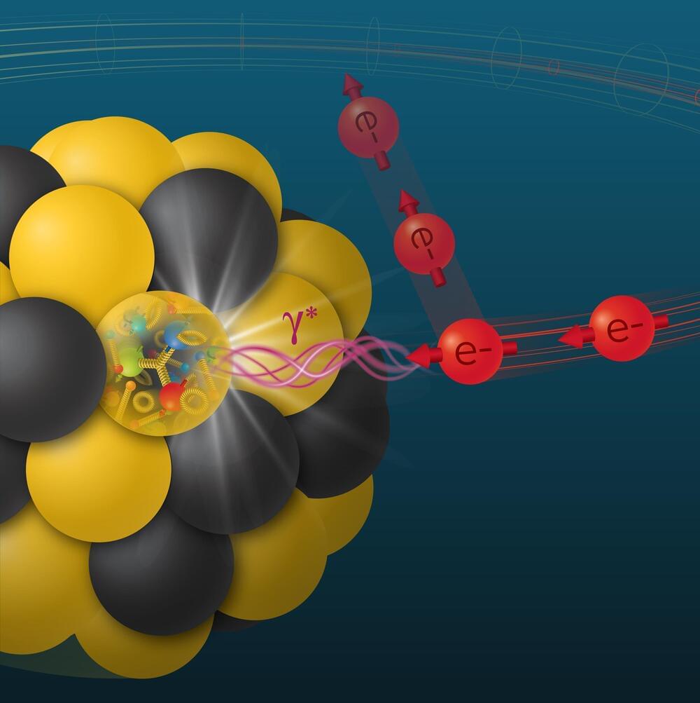
Scientists calculate predictions for meson measurements
Nuclear physics theorists at the U.S. Department of Energy’s (DOE) Brookhaven National Laboratory have demonstrated that complex calculations run on supercomputers can accurately predict the distribution of electric charges in mesons, particles made of a quark and an antiquark. Scientists are keen to learn more about mesons—and the whole class of particles made of quarks, collectively known as hadrons—in high-energy experiments at the future Electron-Ion Collider (EIC), a particle collider being built at Brookhaven Lab.
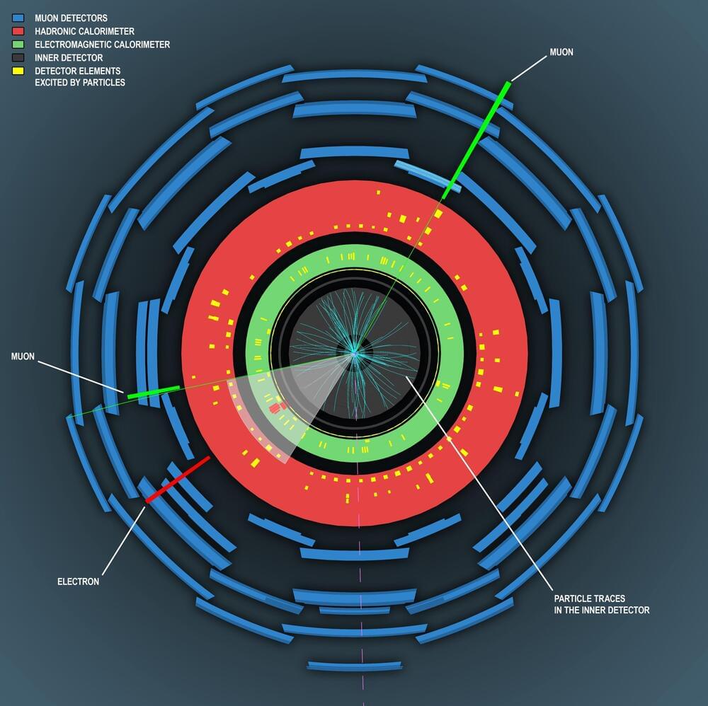
Can unknown physics be seen in interactions between Higgs bosons?
Since the launch of the Large Hadron Collider, there has been ongoing research there into Higgs bosons and a search for traces of physics beyond the existing model of elementary particles. Scientists working at the ATLAS detector have combined both goals: with the latest analysis it has been possible to expand our knowledge of the interactions of Higgs bosons with each other, and stronger constraints on the phenomena of “new physics” have been found.