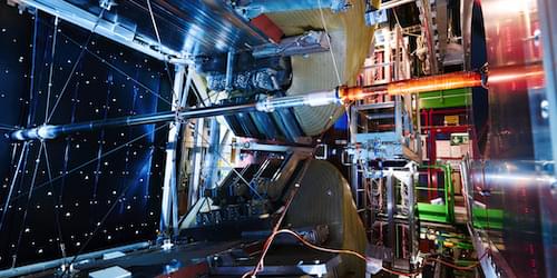
Does a new measurement of a rare decay of the neutral B meson portend new physics?
In particle physics, ten years is a long time to sit with a puzzle. Since 2013, measurements of a rare decay—a neutral B meson (B0) transforming into an excited kaon (K*0) and a muon–antimuon pair (µ+µ –)—have stubbornly refused to match the predictions of the standard model, the theory that describes all known particles and forces [1]. Small enough to be dismissed at first as a statistical fluctuation, the pattern of discrepancies has grown with each new dataset into one of the most tantalizing hints of new physics in experimental particle physics. Now the LHCb Collaboration at CERN in Switzerland has published its most comprehensive analysis of the decay to date [2]. The result is clear: The anomaly persists. Encouragingly, the theoretical and experimental tools to understand it have never been sharper.
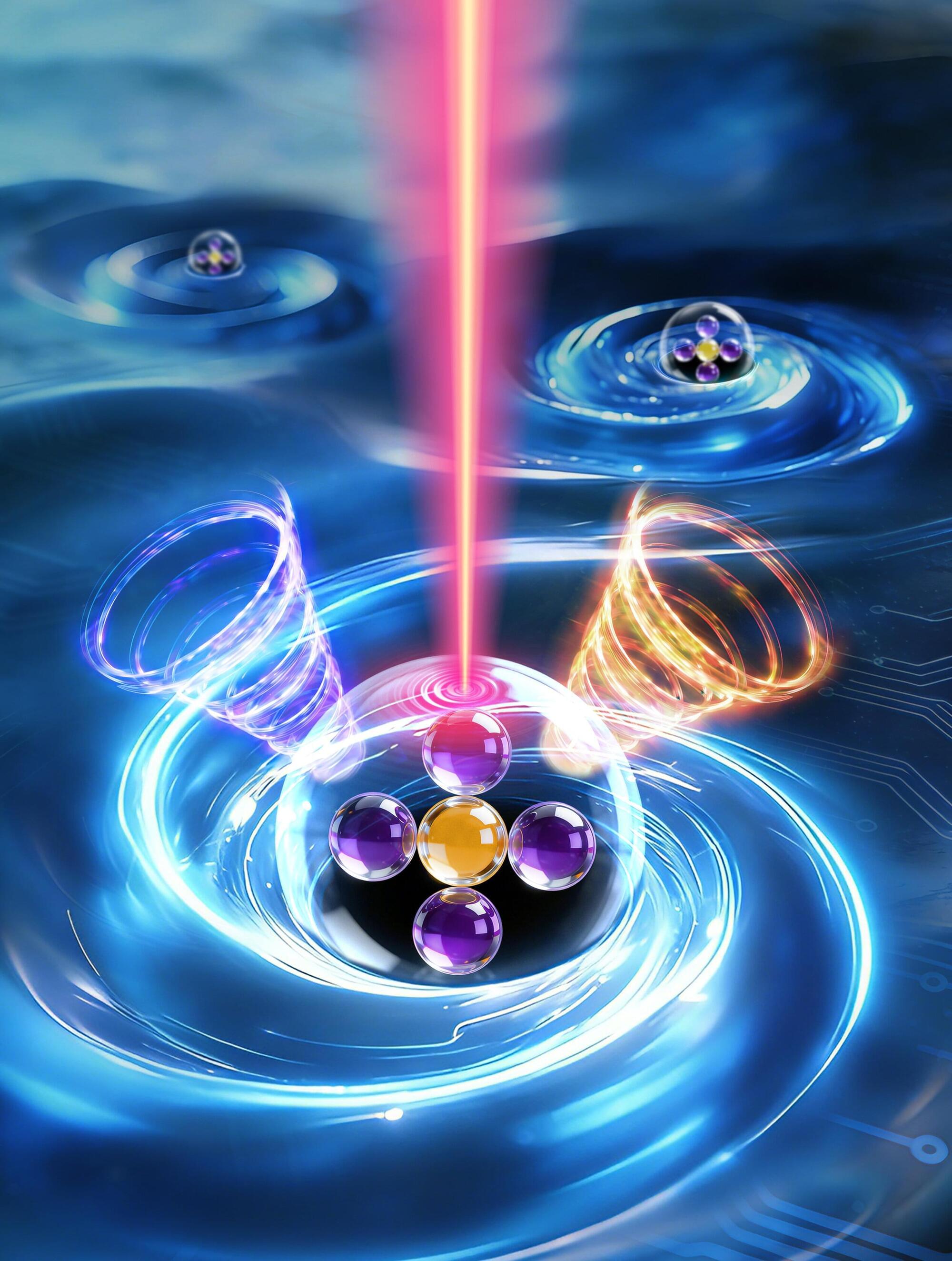
Within the mathematical framework of the standard model, the decay in question, B0  → K*0µ+µ–, can occur only through so-called higher-order electroweak loop diagrams in which a bottom, or b, quark transforms into a strange, or s, quark [3]. As a result, the decay is extraordinarily rare. In every million B-meson decays of all kinds, you can expect to find only one. That rarity makes the decay valuable: It could bear measurable imprints of particles beyond the standard model that contribute to the same loop processes but have so far escaped detection because they are too heavy.

