Once described by Einstein as “spooky action at a distance,” quantum entanglement may now seem less intimidating in light of new research findings.
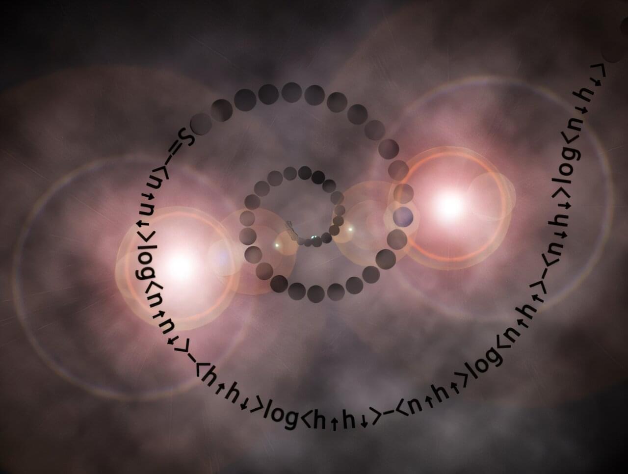
Osaka Metropolitan University physicists have developed new, simpler formulas to quantify quantum entanglement in strongly correlated electron systems and applied them to study several nanoscale materials. Their results offer fresh perspectives into quantum behaviors in materials with different physical characteristics, contributing to advances in quantum technologies.
Oxygen is essential for life and a reactive player in many chemical processes. Accordingly, methods that accurately measure oxygen are relevant for numerous industrial and medical applications: They analyze exhaust gases from combustion processes, enable the oxygen-free processing of food and medicines, monitor the oxygen content of the air we breathe or the oxygen saturation in blood.
“However, such measurements usually require bulky, power-hungry, and expensive devices that are hardly suitable for mobile applications or continuous outdoor use,” says Máté Bezdek, Professor of Functional Coordination Chemistry at ETH Zurich. His group uses molecular design methods to find new sensors for environmental gases.
Early diagnosis is crucial in disease prevention and treatment. Many diseases can be identified not just through physical signs and symptoms but also through changes at the cellular and molecular levels.
When it comes to a majority of chronic conditions, early detection, particularly at the cellular level, gives patients a better chance for successful treatment. Detection of early changes at the cellular level can also dramatically improve cancer outcomes.
It’s against this backdrop that a University of Rhode Island professor and a former Ph.D. graduate student looked at understanding the smallest changes between two similar cells.
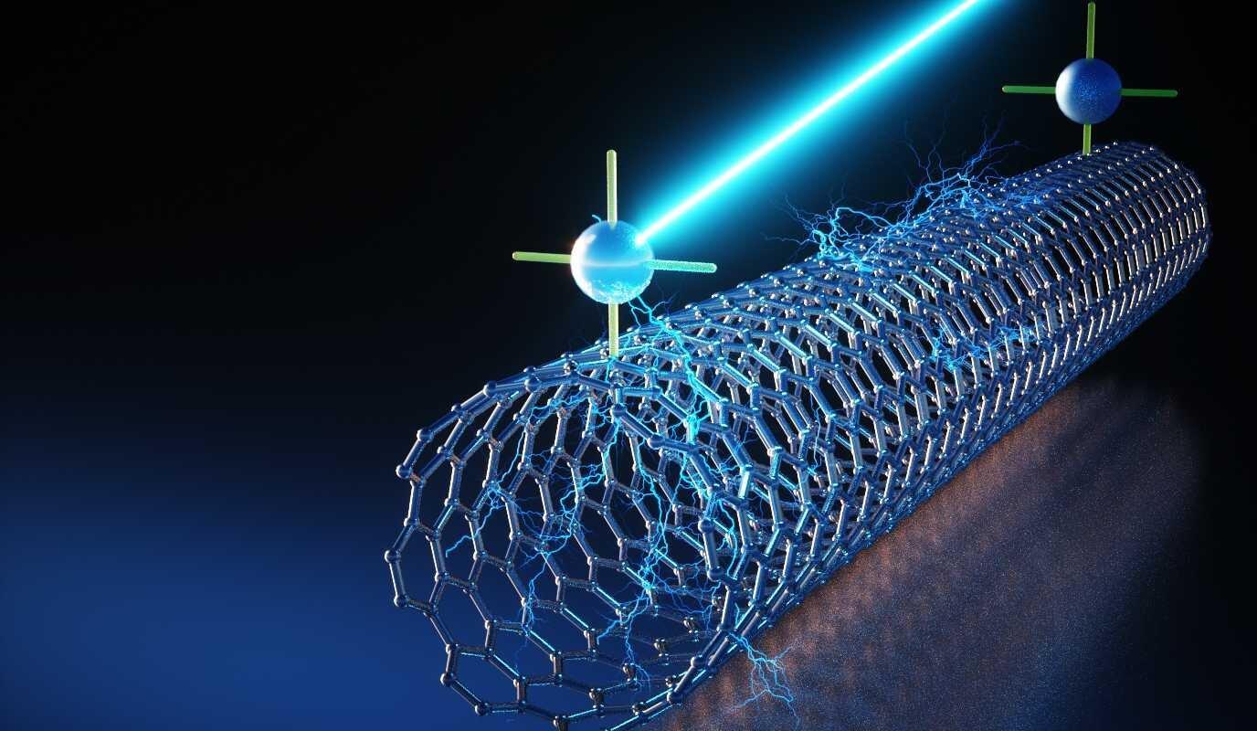
Getting seven experiments on the International Space Station requires a really good idea. Like a brand new way to attack tumors—one that you can only make in space.
Space has unique advantages for making medicines. Its very low gravity makes it possible to grow molecules in shapes and uniformity that are difficult to create on Earth. If they can be reliably and affordably produced, such molecules could have all kinds of novel uses in industry and medicine.
University of Connecticut engineer Yupeng Chen has been growing one such unusually rod-shaped nanoparticle, called a Janus base nanotube, on the International Space Station (ISS).
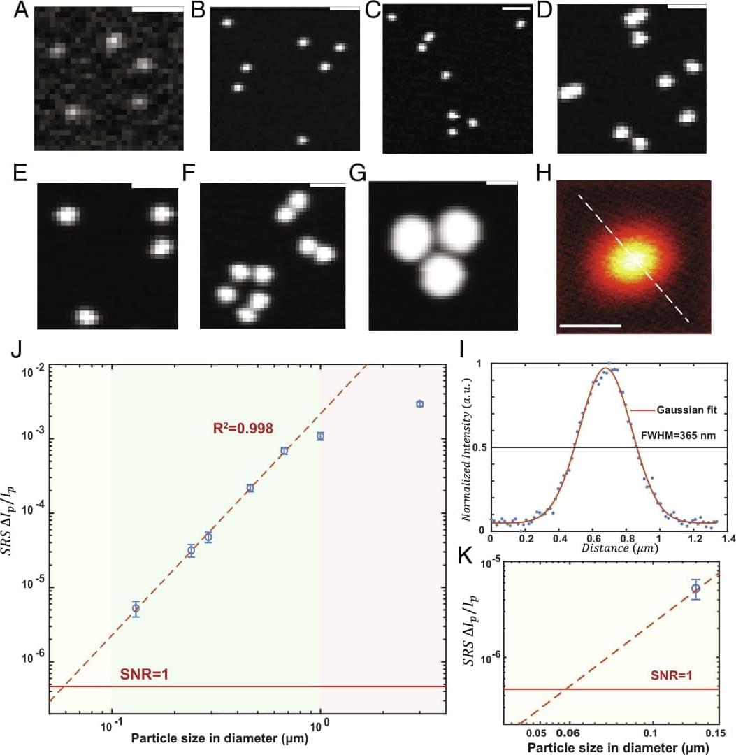
The shape is another important morphological feature that matters as a critical aspect of nanotoxicity. Studies have shown that shape plays a role in determining the cellular uptake of micro-nano particles (65, 66). SRS images of plastic particles confirmed the existence of shape diversity for micro-nano plastics in bottled water. To account for the shape of plastic particles in a statistical manner, we measure the aspect ratio of individual particles above the diffraction limit (Fig. 6 H). The aspect ratio is widely acknowledged in nanotoxicology studies (67, 68). The aspect ratio of the plastic particles detected ranges from 1 to 6, and the average aspect ratio for particles is around 1.7. Fig. 6 I–M provides a pictorial view of how the aspect ratio is related to the particle shape. Particles with an aspect ratio of above 3 are most likely to be fibrous in shape, while particles with an aspect ratio of below 1.4 will be largely spherical. Shape variation on plastic particles has been found in all polymers detected, confirming the widely recognized idea that real-world micro-nano plastics have diverse morphological prosperities. This dimension is hard to be resembled by engineered polymer nanoparticles commonly studied in research laboratories, and the toxicological consequences pertaining to real-life plastic particle exposures and their differing physicochemical properties (i.e., size, shape) have yet to be determined.
Getting seven experiments on the International Space Station requires a really good idea. Like a brand new way to attack tumors—one that you can only make in space.
Space has unique advantages for making medicines. Its very low gravity makes it possible to grow molecules in shapes and uniformity that are difficult to create on Earth. If they can be reliably and affordably produced, such molecules could have all kinds of novel uses in industry and medicine.
University of Connecticut engineer Yupeng Chen has been growing one such unusually rod-shaped nanoparticle, called a Janus base nanotube, on the International Space Station (ISS). The success of Chen’s last five experiments has led to this latest $1.9 million award from the Center for Advancement of Science in Space and NASA’s Division of Biological and Physical Sciences. With it, Chen and his colleagues will use the space station’s unique environment to grow pharmaceuticals whose shape is their secret weapon.#
Experiments aboard the International Space Station may offer promising advancements in fighting cancer.
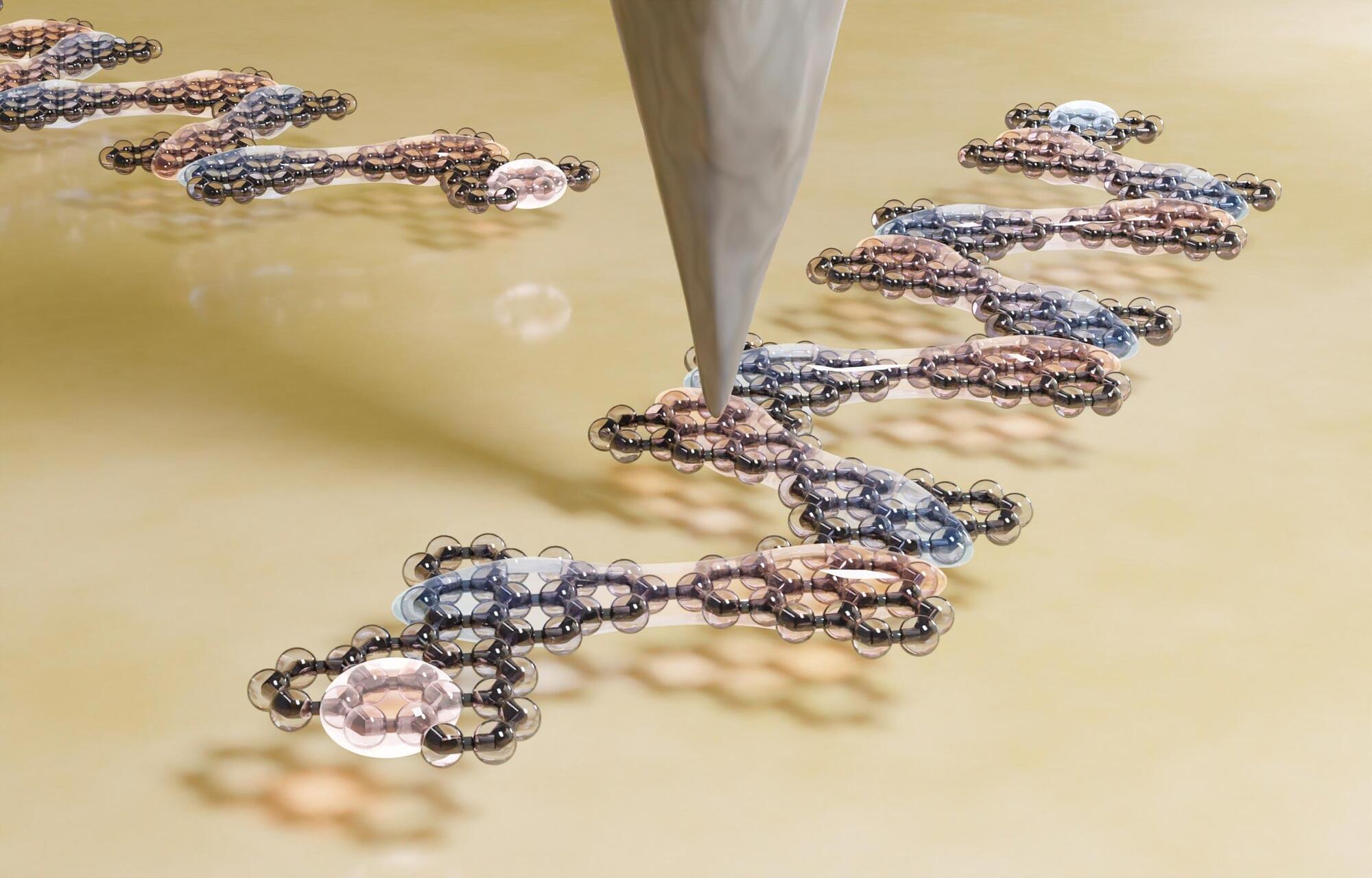
However, as with much of quantum physics, this “language”—the interaction between spins—is extraordinarily complex. While it can be described mathematically, solving the equations exactly is nearly impossible, even for relatively simple chains of just a few spins. Not exactly ideal conditions for turning theory into reality…
A model becomes reality
Researchers at Empa’s nanotech@surfaces laboratory have now developed a method that allows many spins to “talk” to each other in a controlled manner – and that also enables the researchers to “listen” to them, i.e. to understand their interactions. Together with scientists from the International Iberian Nanotechnology Laboratory and the Technical University of Dresden, they were able to precisely create an archetypal chain of electron spins and measure its properties in detail. Their results have now been published in the renowned journal Nature Nanotechnology.
For our Medical Nanobots, in 5 to 10 years, once they are ready to go and wipe out all diseases.
Some bacteria deploy tiny spearguns to retaliate against rival attacks. Researchers at the University of Basel mimicked attacks by poking bacteria with an ultra-sharp tip. Using this approach, they have uncovered that bacteria assemble their nanoweapons in response to cell envelope damage and rapidly strike back with high precision.
The hosts discuss the 2014 film Transcendence by Wally Pfister and Jack Paglen. It depicts a world grappling with the implications of advanced artificial intelligence. The narrative follows a brilliant scientist whose consciousness is uploaded into a powerful computer system, leading to rapid technological advancements and sparking both hope and fear in humanity. As this AI evolves, questions arise about its intentions, its impact on society, and the very definition of life and consciousness, creating escalating conflict and raising profound ethical dilemmas. The screenplay excerpts depict a world grappling with the implications of advanced Artificial Intelligence (AI) and nanotechnology, touching upon several ethical topics. Dr. Max Waters, an AI researcher, is central to the narrative. There’s evidence of mind uploading or the transfer of consciousness to machines, particularly concerning a character named Will (Johnny Depp). This raises fundamental ethical questions about the nature of consciousness, the definition of life, and the potential for a digital consciousness.
The development of a powerful AI and the proliferation of nanotechnology appear to lead to a technological singularity, a point where technological growth becomes uncontrollable and irreversible, raising fears of a dystopian future and tech gone wrong. An organization called the RIFT opposes this technological advancement, highlighting the ethical concerns surrounding uncontrolled technological progress.
The screenplay also features conflict and threats, suggesting the potential for misuse of advanced technology and raising questions about its impact on humanity. The involvement of the FBI indicates that this technology poses a significant threat to societal order. Furthermore, the presence of a computer virus as a plot device suggests the vulnerabilities and risks associated with highly interconnected technological systems. The narrative explores the complex ethical dilemmas arising from the creation of highly intelligent machines and the transformative power of nanotechnology, including the potential loss of human autonomy and the unpredictable consequences of the AISingularity. #artificialintelligence #Transcendence #SciFiThriller #AISingularity #Nanotechnology #MindUploading #FutureTech #DystopianFuture #TechGoneWrong #Consciousness #MovieScreenplay #ScienceFiction #TechnologicalSingularity #AI