Toggle light / dark theme

Precisely controlled levitation of nanodiamonds could bring advances in sensors, quantum information processing

Researchers have demonstrated how to control the “electron spin” of a nanodiamond while it is levitated with lasers in a vacuum, an advance that could find applications in quantum information processing, sensors and studies into the fundamental physics of quantum mechanics.

Electrons can be thought of as having two distinct spin states, “up” or “down.” The researchers were able to detect and control the electron spin resonance, or its change from one state to the other.

“We’ve shown how to continuously flip the electron spin in a nanodiamond levitated in a vacuum and in the presence of different gases,” said Tongcang Li, an assistant professor of physics and astronomy and electrical and computer engineering at Purdue University.

Electron spin control: Levitated nanodiamond is research gem

I’m telling folks there is much to be learn in the usage of natural and synthetic resources especially around diamonds — Nanodiamonds Magic.


WEST LAFAYETTE, Ind. — Researchers have demonstrated how to control the “electron spin” of a nanodiamond while it is levitated with lasers in a vacuum, an advance that could find applications in quantum information processing, sensors and studies into the fundamental physics of quantum mechanics.

Electrons can be thought of as having two distinct spin states, “up” or “down.” The researchers were able to detect and control the electron spin resonance, or its change from one state to the other.

“We’ve shown how to continuously flip the electron spin in a nanodiamond levitated in a vacuum and in the presence of different gases,” said Tongcang Li, an assistant professor of physics and astronomy and electrical and computer engineering at Purdue University.

World’s Smallest Hard Drive Writes Data Atom-By-Atom

Meet the world’s smallest hard drive.


Dutch scientists have developed a unique solution to deal with the data storage problem. By manipulating single atoms, researchers have created the world’s smallest hard drive capable of storing 1 kilobyte of data (8000 bits) in a space under 100 nanometers across. The technology means that all the books in the world could be stored on a device the size of a postage stamp.

In a study published Monday in the journal Nature Nanotechnology, scientists from the Technical University of Delft (TU Delft) said that they have created an atomic hard drive with a storage density that is 500 times greater than current hard drive technology.

Associate Professor at TU Delft and lead researcher Sander Otte and his team found that placing chlorine atoms on a copper surface created the perfect square grid. A hole appears in the grid when an atom is missing. Using a scanning tunneling microscope, scientists were able to move atoms around one by one and even drag individual atoms toward the hole.

Scientists develop way to upsize nanostructures into light, flexible 3D printed materials

For years, scientists and engineers have synthesized materials at the nanoscale level to take advantage of their mechanical, optical, and energy properties, but efforts to scale these materials to larger sizes have resulted in diminished performance and structural integrity.

Now, researchers led by Xiaoyu “Rayne” Zheng, an assistant professor of mechanical engineering at Virginia Tech have published a study in the journal Nature Materials that describes a new process to create lightweight, strong and super elastic 3D printed metallic nanostructured with unprecedented scalability, a full seven orders of magnitude control of arbitrary 3D architectures.

Strikingly, these multiscale metallic materials have displayed super elasticity because of their designed hierarchical 3D architectural arrangement and nanoscale hollow tubes, resulting in more than a 400 percent increase of tensile elasticity over conventional lightweight metals and ceramic foams.

‘Green’ electronic materials produced with synthetic biology

Biowire.


Researchers led by microbiologist Derek Lovely say the wires, which rival the thinnest wires known to man, are produced from renewable, inexpensive feedstocks and avoid the harsh chemical processes typically used to produce nanoelectronic materials.

Lovley says, “New sources of electronic materials are needed to meet the increasing demand for making smaller, more powerful electronic devices in a sustainable way.” The ability to mass-produce such thin conductive wires with this sustainable technology has many potential applications in electronic devices, functioning not only as wires, but also transistors and capacitors. Proposed applications include biocompatible sensors, computing devices, and as components of solar panels.

This advance began a decade ago, when Lovley and colleagues discovered that Geobacter, a common soil microorganism, could produce “microbial nanowires,” electrically conductive protein filaments that help the microbe grow on the iron minerals abundant in soil. These microbial nanowires were conductive enough to meet the bacterium’s needs, but their conductivity was well below the conductivities of organic wires that chemists could synthesize.

New Technique Developed for Effective Dye Removal and Low-Cost Water Purification

Purifying H2O more cheaply.


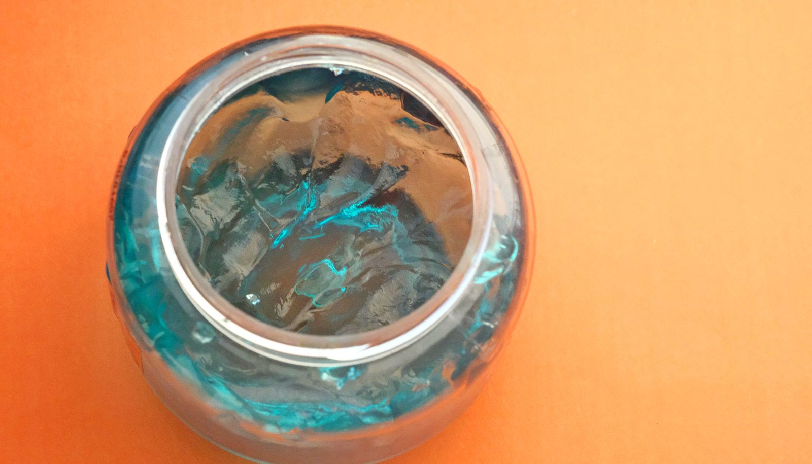
WASHINGTON—()—Organic compounds in wastewater, such as dyes and pigments in industry effluents, are toxic or have lethal effect on aquatic living and humans. Increasing evidence has shown that the organic contaminants discharged from electroplating, textile production, cosmetics, pharmaceuticals are the main reasons for the higher morbidity rates of kidney, liver, and bladder cancers, etc. Organic contaminants, especially methyl blue and methyl orange, are stable to light, heat or oxidizing agents and very difficult to remove by conventional chemical or biological wastewater treatment techniques. Recently scientists have developed some new strategies with good dye-removal performance; however, a subsequent adsorbent purification procedure is unavoidable after water treatment, which are often complicated and not suitable for practical water treatment.

Now, using laser-induced fabrication technique, a team of Chinese researchers from Shandong University, China, have developed a novel dye adsorbent. Hybrid nano-particles of silver and silver sulfide (Ag2S@Ag hybrid nano-particles) have demonstrated the nanomaterial’s superior adsorption performance for removing methyl blue and methyl orange from wastewater. More importantly, the new adsorbents can be removed directly from solutions by filters without adsorbent purification procedures, as the silver-based hybrid nano-particles will be agglomerated and deposited on the bottom after adsorbing dyes, providing a green, simple, rapid and low-cost solution for water purification. This week in the journal Optical Materials Express, from The Optical Society (OSA), the researchers describe the work.

‘Smart’ thread collects diagnostic data when sutured into tissue

Way cool! Your stitches monitors and reports your progress to your doctor/s.

BTW — In 1999, I told a guy from Diamond Intl. that the thread in our clothing would be able to do this in the next 15 to 20 years. He laughed at me; never say never.


For the first time, researchers led by Tufts University engineers have integrated nano-scale sensors, electronics and microfluidics into threads — ranging from simple cotton to sophisticated synthetics — that can be sutured through multiple layers of tissue to gather diagnostic data wirelessly in real time, according to a paper published online July 18 in Microsystems & Nanoengineering. The research suggests that the thread-based diagnostic platform could be an effective substrate for a new generation of implantable diagnostic devices and smart wearable systems.

The researchers used a variety of conductive threads that were dipped in physical and chemical sensing compounds and connected to wireless electronic circuitry to create a flexible platform that they sutured into tissue in rats as well as in vitro. The threads collected data on tissue health (e.g. pressure, stress, strain and temperature), pH and glucose levels that can be used to determine such things as how a wound is healing, whether infection is emerging, or whether the body’s chemistry is out of balance. The results were transmitted wirelessly to a cell phone and computer.

The three-dimensional platform is able to conform to complex structures such as organs, wounds or orthopedic implants.

Is invisibility cloak on its way to reality?

Invisibility cloak has hidden Harry Potter and hobbits from view and now, this sci-fi staple may be moving closer to reality!

Scientists at Queen Mary University of London (QMUL) have made an object disappear by using a composite material with nano-size particles that can enhance specific properties on the object’s surface.

Researchers demonstrated for the first time a practical cloaking device that allows curved surfaces to appear flat to electromagnetic waves.

Images made of relativistic electrons trapped in graphene quantum dots

(Phys.org)—A team of researchers with the University of California, MIT, Lawrence Berkeley National Laboratory and the National Institute for Materials Science in Japan has created images of relativistic electrons trapped in graphene quantum dots. In their paper published in the journal Nature Physics the team describes how they achieved this feat and where they plan to take their work in the future.

As the many unique properties of graphene continue to unfold, scientists seek new ways to harness and eventually make use of them. One such use might be to control electrons to allow their use in nano-scaled devices, which could also inadvertently lead to a deeper understanding of Dirac fermions. In this new effort, the researchers have made progress in that area by devising a means for capturing and holding electrons and for creating images of the result.

Obtaining images of electron waveforms has thus far been particularly difficult—virtually all existing methods have resulted in too many defects. To get around such problems, the researchers took another approach to capturing the electrons. They first created circular p-n junctions by sending voltage through the tip of a scanning tunneling microscope down to a graphene sample below. At the same time, they also applied voltage to a slab of silicon underneath the piece of graphene, which was kept separated by a layer of silicon-oxide and a flake of . Doing so caused defects in the boron nitride to ionize, resulting in charges migrating to the graphene.

/* */