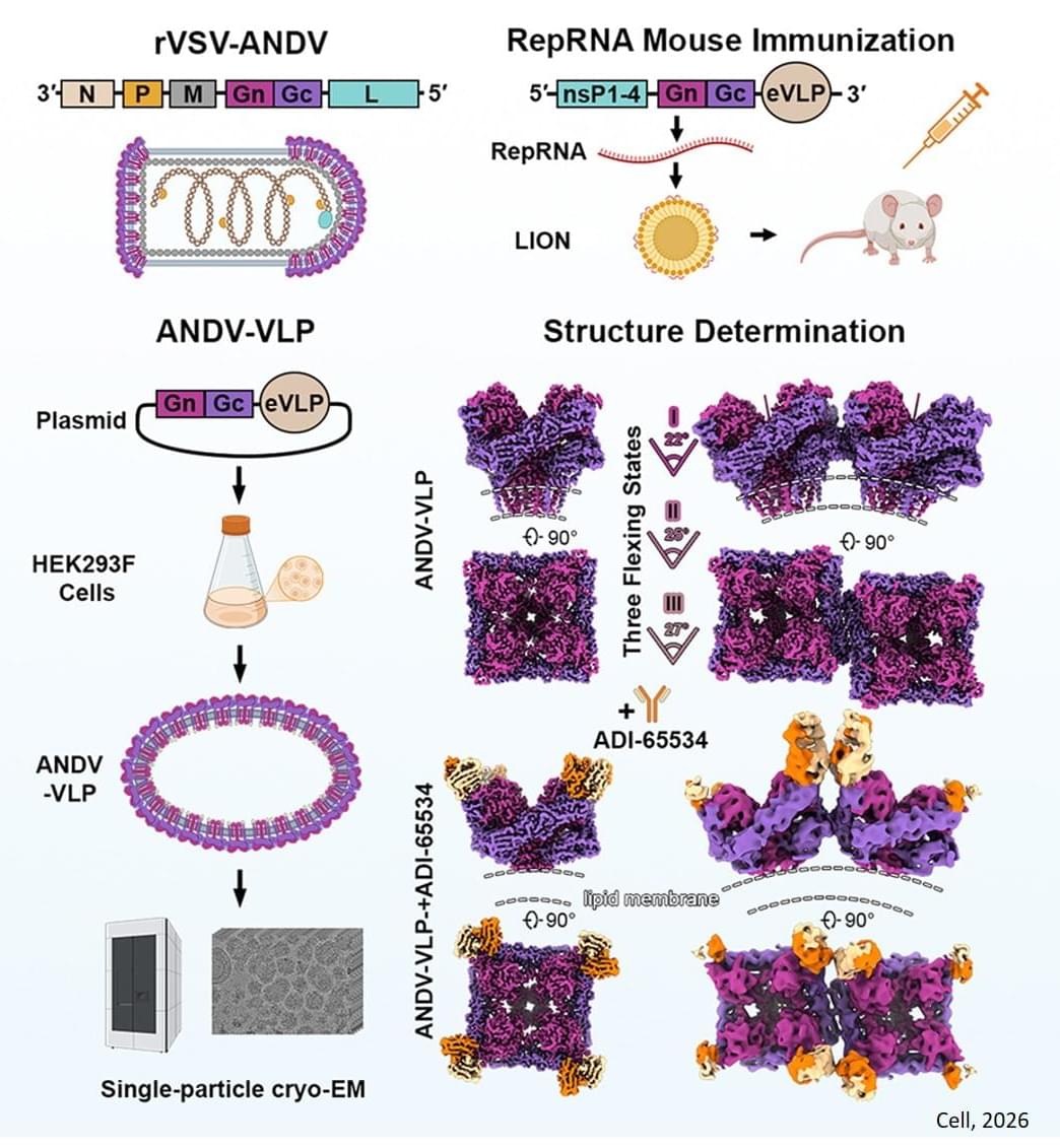
Toggle light / dark theme

A team from Lawrence Livermore National Laboratory, Stanford University and the University of Pennsylvania introduced a novel wet chemical etching process that modifies the surface of conventional metal powders used in 3D printing.


In a significant advancement for metal additive manufacturing, researchers at Lawrence Livermore National Laboratory (LLNL) and their academic partners have developed a groundbreaking technique that enhances the optical absorptivity of metal powders used in 3D printing.

The innovative approach, which involves creating nanoscale surface features on metal powders, promises to improve the efficiency and quality of printed metal parts, particularly for challenging materials like copper and tungsten, according to researchers.

Additive manufacturing (AM) — more commonly known as 3D printing — has transformed the way products are designed and produced, allowing for the creation of complex geometries and customized components that traditional manufacturing methods struggle to achieve. However, one of the persistent challenges in laser powder-bed fusion (LPBF) metal 3D printing is the high reflectivity of certain metals, which can lead to inefficient energy absorption during the printing process and can even damage some printing machines. This inefficiency often results in inadequate print quality and increased energy consumption, according to researchers.

This study presents the development and characterization of a novel nanocomposite wound dressing material based on polylactic acid (PLA) nanofibers incorporating chitosan nanocapsules loaded with chamomile extract and cellulose nanoparticles.


Asadzadeh, F., Ghorbanzadeh, S., Poursattar Marjani, A. et al. Sci Rep 14, 22,336 (2024). https://doi.org/10.1038/s41598-024-72398-9

Download citation.

Using a nanoscale structure that consisted of a sequential array of a source electrode, a quantum well, a tunneling barrier, a quantum dot, another tunneling barrier, and a drain electrode, researchers were able to suppress electron excitation and cool electrons to −228 °C (−378 °F) without external means at room temperature.

A team of researchers has discovered a way to cool electrons to −228 °C without external means and at room temperature, an advancement that could enable electronic devices to function with very little energy.

The process involves passing electrons through a quantum well to cool them and keep them from heating.

Brookhaven National Laboratory researchers are working to develop ways to synchronize the magnetic spins in nanoscale devices to build tiny signal-generating or receiving antennas and other electronics.

Upton, New York — Scientists at the U.S. Department of Energy’s Brookhaven National Laboratory are seeking ways to synchronize the magnetic spins in nanoscale devices to build tiny yet more powerful signal-generating or receiving antennas and other electronics. Their latest work, published in Nature Communications, shows that stacked nanoscale magnetic vortices separated by an extremely thin layer of copper can be driven to operate in unison, potentially producing a powerful signal that could be put to work in a new generation of cell phones, computers, and other applications.

The aim of this “spintronic” technology revolution is to harness the power of an electron’s “spin,” the property responsible for magnetism, rather than its negative charge.

A new study from researchers at Tyndall National Institute and the National University of Singapore shows that subtle changes in the intermolecular van der Waals interactions in the active component of a molecular diode can improve the device performance by more than a factor of ten.

A team of scientists from Tyndall National Institute at University College Cork and the National University of Singapore have designed and fabricated ultra-small devices for energy-efficient electronics. By finding out how molecules behave in these devices, a ten-fold increase in switching efficiency was obtained by changing just one carbon atom. These devices could provide new ways to combat overheating in mobile phones and laptops, and could also aid in electrical stimulation of tissue repair for wound healing. The breakthrough creation of molecular devices with highly controllable electrical properties will appear in the February issue of Nature Nanotechnology. Dr. Damien Thompson at the Tyndall National Institute, UCC and a team of researchers at the National University of Singapore led by Prof. Chris Nijhuis designed and created the devices, which are based on molecules acting as electrical valves, or diode rectifiers.

Dr. Thompson explains “These molecules are very useful because they allow current to flow through them when switched ON and block current flow when switched OFF. The results of the study show that simply adding one extra carbon is sufficient to improve the device performance by more than a factor of ten. We are following up lots of new ideas based on these results, and we hope ultimately to create a range of new components for electronic devices.” Dr. Thompson’s atom-level computer simulations showed how molecules with an odd number of carbon atoms stand straighter than molecules with an even number of carbon atoms. This allows them to pack together more closely. Tightly-packed assemblies of these molecules were formed on metal electrode surfaces by the Nijhuis group in Singapore and were found to be remarkably free of defects. These high quality devices can suppress leakage currents and so operate efficiently and reliably.

A collaborative research team has developed a novel method to measure minuscule nanoscale forces in liquids, using a technique that significantly enhances measurement sensitivity and resolution. This breakthrough could transform biological research and advance biomedical technology.

Groundbreaking research has introduced a new method for measuring extremely small forces at the nanoscale within aqueous environments, expanding our understanding of the microscopic realm.

The significant nanotechnology advance was achieved by researchers from Beihang University in China with RMIT University and other leading institutions including the Australian National University and University of Technology Sydney.

Researchers at the Fritz Haber Institute have advanced nanoscale optoelectronics by developing a method to control single-molecule photoswitching with atomic precision.

This method utilizes localized surface plasmons on semiconductor platforms to precisely adjust molecular configurations, enhancing device efficiency and adaptability. This innovation promises significant improvements in the miniaturization and functionality of future electronic and photonic devices, potentially impacting a wide range of applications including sensors and photovoltaic cells.

Groundbreaking Discovery in Nanoscale Optoelectronics.

New research from North Carolina State University shows that unique materials with distinct properties akin to those of gecko feet – the ability to stick to just about any surface – can be created by harnessing liquid-driven chaos to produce soft polymer microparticles with hierarchical branching on the micro-and nanoscale.

The findings, published today (October 14, 2019) in the journal Nature Materials, hold the potential for advances in gels, pastes, foods, nonwovens, and coatings, among other formulations.

The soft dendritic particle materials with unique adhesive and structure-building properties can be created from a variety of polymers precipitated from solutions under special conditions, says Orlin Velev, S. Frank and Doris Culberson Distinguished Professor of Chemical and Biomolecular Engineering at NC State and corresponding author of the paper.