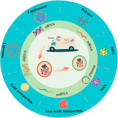
Toggle light / dark theme

Deep Nanometry: Deep learning system detects disease-related nanoparticles

Researchers, including those from the University of Tokyo, developed Deep Nanometry, an analytical technique combining advanced optical equipment with a noise removal algorithm based on unsupervised deep learning.

Deep Nanometry can analyze nanoparticles in medical samples at high speed, making it possible to accurately detect even trace amounts of rare particles. This has proven its potential for detecting indicating early signs of colon cancer, and it is hoped that it can be applied to other medical and industrial fields.

The body is full of smaller than cells. These include extracellular vesicles (EVs), which can be useful in early disease detection and also in drug delivery.

Self-driving lab transforms electronic polymers discovery

Plastic that conducts electricity might sound impossible. But there is a special class of materials known as “electronic polymers” that combines the flexibility of plastic with the functionality of metal. This type of material opens the door for breakthroughs in wearable devices, printable electronics and advanced energy storage systems.

Yet, making thin films from electronic polymers has always been a difficult task. It takes a lot of fine-tuning to achieve the right balance of physical and . Researchers at the U.S. Department of Energy’s (DOE) Argonne National Laboratory have created an innovative solution to this challenge with artificial intelligence (AI).

They used an AI-driven, automated materials laboratory, a tool called Polybot, to explore processing methods and produce high-quality films. Polybot is located at the Center for Nanoscale Materials, a DOE Office of Science user facility at Argonne.

Solid state lubricant uses atomically thin sheets to achieve extremely low friction

Finding the right lubricant for the right purpose is a task that is often extremely important in industry. Not only to reduce friction, overheating and wear, but also to save energy. At TU Wien, the research groups of Prof Carsten Gachot (Tribology, Mechanical Engineering) and Prof Dominik Eder (Chemistry) are therefore working together to develop innovative, improved lubricants.

The team has now presented a new type of material with special properties: The lubricant COK-47 is not liquid like lubricating oil, but a powdery solid substance. On a nanoscale, it consists of stacks of atomically thin sheets, like a tiny stack of cards.

When the material comes into contact with , these platelets can slide past each other very easily—a so-called tribofilm is created, which ensures extremely low . This makes COK-47 a highly interesting in .

Microfluidic component library component library enables rapid, low-cost device prototyping

Researchers have developed a freely available droplet microfluidic component library, which promises to transform the way microfluidic devices are created. This innovation, based on low-cost rapid prototyping and electrode integration, makes it possible to fabricate microfluidic devices for under $12 each, with a full design-build-test cycle completed within a single day. The components are biocompatible, high-throughput, and capable of performing multistep workflows, such as droplet generation, sensing, sorting, and anchoring, all critical for automating microfluidic design and testing.

Microfluidics, particularly droplet-based systems, has become a promising technology for diverse fields, including protein engineering, single-cell sequencing, and nanoparticle synthesis. However, the traditional methods of fabricating —typically using PDMS (polydimethylsiloxane)—are time-consuming and costly, often requiring cleanroom facilities or external vendors.

While alternatives like laser cutting and 3D printing have been explored, these methods often suffer from limitations in resolution, material compatibility, and scalability. As a result, there has been an urgent need for a more efficient, cost-effective, and accessible fabrication method to help propel innovation in microfluidic technology.

Nanoscale technique uses atomic vibrations to show how quantum materials behave at interfaces

Scientists are racing to develop new materials for quantum technologies in computing and sensing for ultraprecise measurements. For these future technologies to transition from the laboratory to real-world applications, a much deeper understanding is needed of the behavior near surfaces, especially those at interfaces between materials.

Scientists at the U.S. Department of Energy’s (DOE) Argonne National Laboratory have unveiled a new technique that could help advance the development of quantum technology. Their innovation, surface-sensitive spintronic (SSTS), provides an unprecedented look at how behave at interfaces.

The work is published in the journal Science Advances.

Breakthrough in High-Performance Fractal Nanowire Photon Detectors

“ tabindex=”0” quantum computing and secure communications. Scientists have optimized materials and processes, making these detectors more efficient than ever.

Revolutionizing Electronics with Photon Detection

Light detection plays a crucial role in modern technology, from high-speed communication to quantum computing and sensing. At the heart of these systems are photon detectors, which identify and measure individual light particles (photons). One highly effective type is the superconducting nanowire single-photon detector (SNSPD). These detectors use ultra-thin superconducting wires that instantly switch from a superconducting state to a resistive state when struck by a photon, enabling extremely fast detection.

Scientists Just Made a Breakthrough in Nanocrystals That Could Supercharge Solar Power

Researchers are breaking new ground with halide perovskites, promising a revolution in energy-efficient technologies.

By exploring these materials at the nanoscale.

The term “nanoscale” refers to dimensions that are measured in nanometers (nm), with one nanometer equaling one-billionth of a meter. This scale encompasses sizes from approximately 1 to 100 nanometers, where unique physical, chemical, and biological properties emerge that are not present in bulk materials. At the nanoscale, materials exhibit phenomena such as quantum effects and increased surface area to volume ratios, which can significantly alter their optical, electrical, and magnetic behaviors. These characteristics make nanoscale materials highly valuable for a wide range of applications, including electronics, medicine, and materials science.