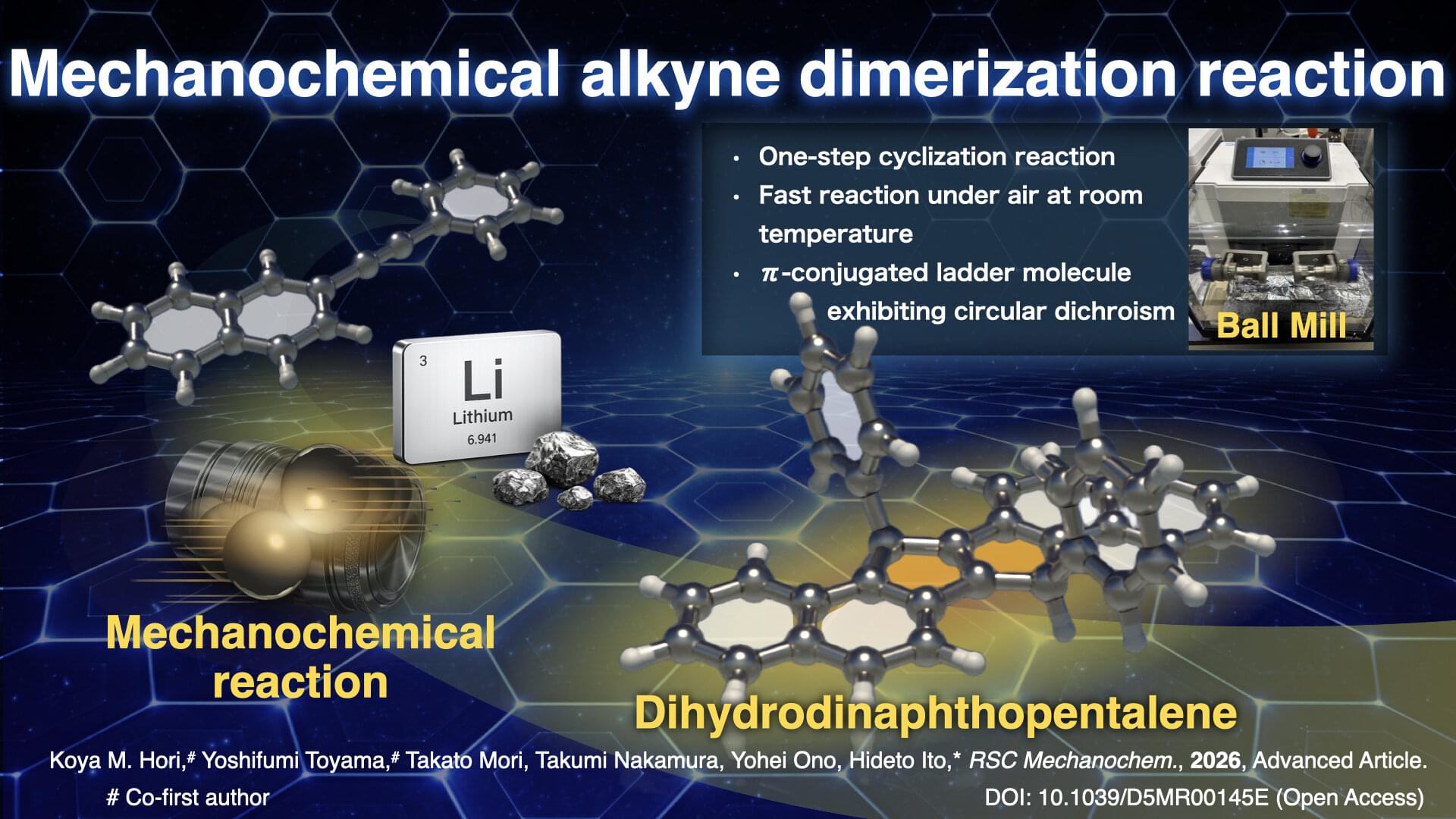
Toggle light / dark theme

A new composite material developed by KIMS researchers absorbs over 99% of electromagnetic waves from different frequencies, improving the performance of devices like smartphones and wearables.

A team of scientists from the Korea Institute of Materials Science (KIMS) has developed the world’s first ultra-thin film composite material capable of absorbing over 99% of electromagnetic waves from various frequency bands, including 5G/6G, WiFi, and autonomous driving radar, using a single material.

This novel electromagnetic wave absorption and shielding material is less than 0.5mm thick and is characterized by its low reflectance of less than 1% and high absorbance of over 99% across three different frequency bands.

Summary: A new AI algorithm inspired by the genome’s ability to compress vast information offers insights into brain function and potential tech applications. Researchers found that this algorithm performs tasks like image recognition and video games almost as effectively as fully trained AI networks.

By mimicking how genomes encode complex behaviors with limited data, the model highlights the evolutionary advantage of efficient information compression. The findings suggest new pathways for developing advanced, lightweight AI systems capable of running on smaller devices like smartphones.

Designed to one day search for evidence of life in the briny ocean beneath the icy shell of Jupiter’s moon Europa, these robots could play a key role in detecting chemical and temperature signals that might indicate alien life, according to scientists at NASA’s Jet Propulsion Laboratory (JPL), who designed and tested the robots.

“People might ask, why is NASA developing an underwater robot for space exploration?” said Ethan Schaler, the project’s principal investigator at JPL. “It’s because there are places we want to go in the solar system to look for life, and we think life needs water.”

Generative AI could saddle the planet with heaps more hazardous waste.

By Saima S. Iqbal

Every time generative artificial intelligence drafts an e-mail or conjures up an image, the planet pays for it. Making two images can consume as much energy as charging a smartphone; a single exchange with ChatGPT can heat up a server so much that it requires a bottle’s worth of water to cool. At scale, these costs soar. By 2027, the global AI sector could annually consume as much electricity as the Netherlands, according to one recent estimate. And a new study in Nature Computational Science identifies another concern: AI’s outsize contribution to the world’s mounting heap of electronic waste. The study found that generative AI applications alone could add 1.2 million to five million metric tons of this hazardous trash to the planet by 2030, depending on how quickly the industry grows.

Money from the CHIPS and Science Act is officially coming to Upstate New York.

GlobalFoundries’ $1.5 billion agreement with the Commerce Department to support expansion plans in Saratoga County and modernization efforts in Vermont has been finalized. The award comes after a Preliminary Memorandum of Terms announced in February.

The award will mainly be used to expand their Malta, New York fab site, adding technology the company already uses in other countries like Germany and Singapore. This will allow them to increase the supply of domestically made computer chips, which are essential in electronic devices from smartphones to aerospace and defense technology.

Scientists have developed a method to improve the stability and efficiency of organic light-emitting diodes (OLEDs), a technology used in smartphones, TVs, and other electronic displays.

This advancement utilizes a unique type of molecule that has the potential to extend the lifespan of OLED devices significantly.

The researchers present a novel way to design that can maintain their stability and efficiency over time, even in high-stress conditions. The research is published in the journal Nature Communications.

Researchers from Seoul National University College of Engineering announced they have developed an optical design technology that dramatically reduces the volume of cameras with a folded lens system utilizing “metasurfaces,” a next-generation nano-optical device.

By arranging metasurfaces on the so that light can be reflected and moved around in the glass substrate in a folded manner, the researchers have realized a with a thickness of 0.7mm, which is much thinner than existing refractive lens systems. The research was published on Oct. 30 in the journal Science Advances.

Traditional cameras are designed to stack multiple glass lenses to refract light when capturing images. While this structure provided excellent high-quality images, the thickness of each lens and the wide spacing between lenses increased the overall bulk of the camera, making it difficult to apply to devices that require ultra-compact cameras, such as virtual and augmented reality (VR-AR) devices, smartphones, endoscopes, drones, and more.

O.o face_with_colon_three


Ctrl-labs is developing an armband that interprets electrical signals from neurons in the arm, allowing wearers to control computers, smartphones, and even robotic arms with their minds. VentureBeat got hands-on time with the technology during a recent visit to the startup’s New York City office.

This robotic Labrador puppy has been created in collaboration with the legendary Jim Henson’s Creature Shop.


A US-based company, Tombot, has unveiled Jennie – a realistic robotic puppy. This battery-powered Lab reacts to human touch, wags its tail, and even barks when you tell it to.

This robotic companion is designed to bring joy and comfort to those who need it most. Jennie has been designed to offer companionship to people battling dementia, stress, anxiety, Posttraumatic Stress Disorder (PTSD), and depression.

Jennie is equipped with various features, including real puppy sounds, software updates, interactive sensors, voice commands, a rechargeable battery, and can be controlled through a smartphone app.