Arranging nonmagnetic atoms on the surface of an unconventional superconductor could induce a novel phenomenon called altermagnetic superconductivity.
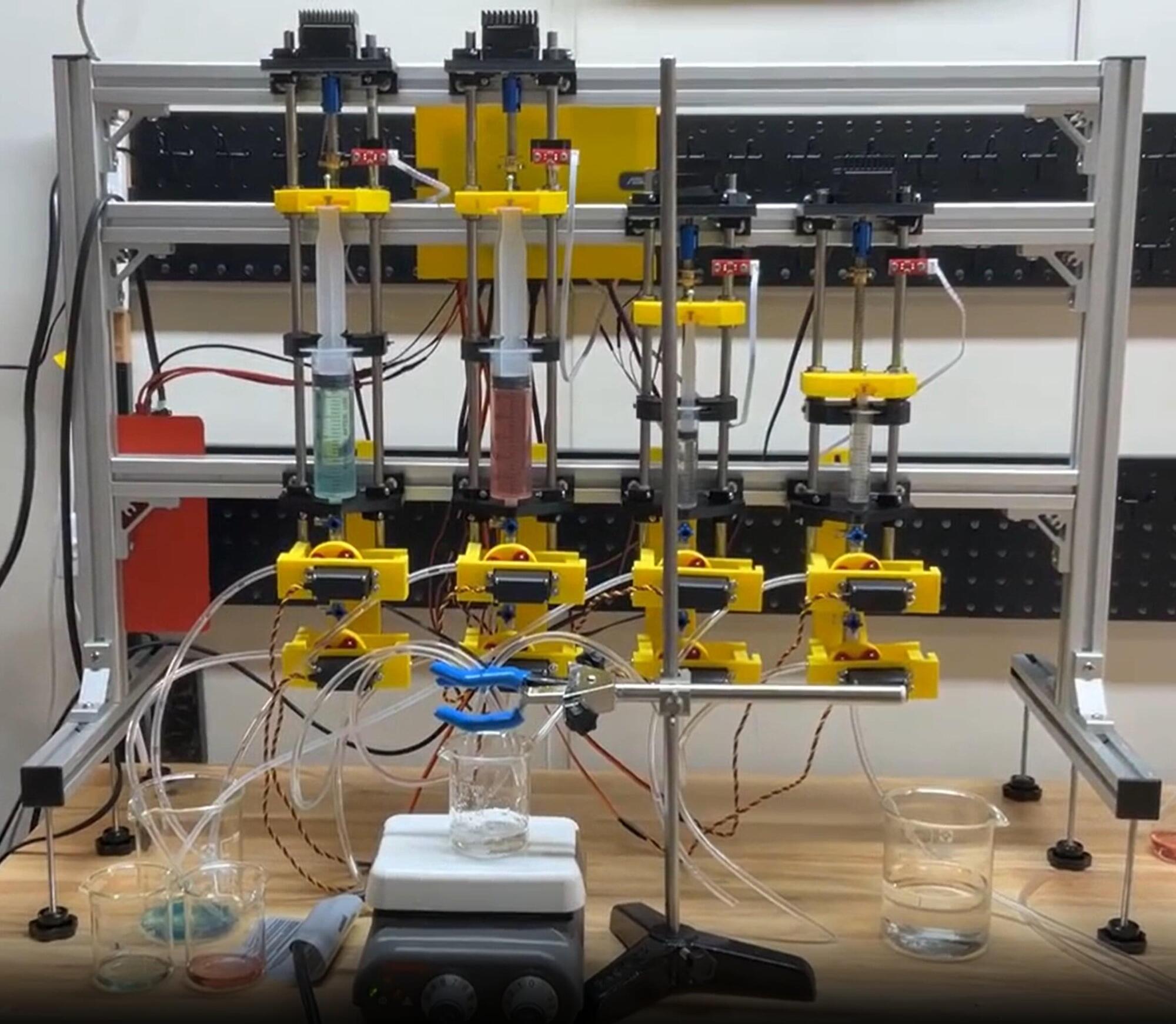
A team of researchers led by Professor Keisuke Takahashi at the Faculty of Science, Hokkaido University, have created FLUID (Flowing Liquid Utilizing Interactive Device), an open-source robotic system constructed using a 3D printer and off-the-shelf electronic components.
To demonstrate FLUID’s capabilities, the team used the robot to automate the co-precipitation of cobalt and nickel, creating binary materials with precision and efficiency.
“By adopting open source, utilizing a 3D printer, and taking advantage of commonly-available electronics, it became possible to construct a functional robot that is customized to a particular set of needs at a fraction of the costs typically associated with commercially-available robots,” said Mikael Kuwahara, the lead author of the study.

University of Warwick astronomers have discovered an extremely rare, high-mass, compact binary star system only ~150 light years away. These two stars are on a collision course to explode as a type 1a supernova, appearing 10 times brighter than the moon in the night sky.
Type 1a supernovae are a special class of cosmic explosion, famously used as “standard candles” to measure distances between Earth and their host galaxies. They occur when a white dwarf (the dense remnant core of a star) accumulates too much mass, is unable to withstand its own gravity, and explodes.
It has long been theoretically predicted that two orbiting white dwarfs are the cause of most type 1a supernova explosions. When in a close orbit, the heavier white dwarf of the pair gradually accumulates material from its partner, which leads to that star (or both stars) exploding.
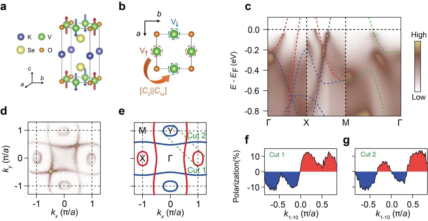
For many years, physics studies focused on two main types of magnetism, namely ferromagnetism and antiferromagnetism. The first type entails the alignment of electron spins in the same direction, while the latter entails the alignment of electron spins in alternating, opposite directions.
Yet recent studies have discovered a new kind of magnetism, referred to as altermagnetism, which does not fit into either of the previously identified categories. Altermagnetism is characterized by the breaking of time-reversal symmetry (i.e., the symmetry of physical laws when time is reversed) and spin-split band structures, in materials that retain a zero net magnetization.
Researchers at the Chinese Academy of Sciences and other institutes in China recently uncovered a new material that exhibits altermagnetism at room temperature, namely KV2Se2O. Their findings, published in Nature Physics, highlight the promise of KV₂Se₂O both for the study of altermagnetism and for the development of spintronic devices.
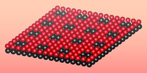
Lacquers, paint, concrete—and even ketchup or orange juice: Suspensions are widespread in industry and everyday life. By a suspension, materials scientists mean a liquid in which tiny, insoluble solid particles are evenly distributed. If the concentration of particles in such a mixture is very high, phenomena can be observed that contradict our everyday understanding of a liquid. For example, these so-called non-Newtonian fluids suddenly become more viscous when a strong force acts upon them. For a brief moment, the liquid behaves like a solid.
This sudden thickening is caused by the particles present in the suspension. If the suspension is deformed, the particles have to rearrange themselves. From an energy perspective, it is more advantageous if they roll past each other whenever possible. It is only when this is no longer possible, e.g., because several particles become jammed, that they have to slide relative to each other. However, sliding requires much more force and thus the liquid feels macroscopically more viscous.
The interactions that occur on a microscopically small scale therefore affect the entire system and they determine how a suspension flows. To optimize the suspension and specifically influence its flow characteristics, scientists must therefore understand the magnitude of the frictional forces between the individual particles.
For centuries, humans have made use of glass in their art, tools, and technology. Despite the ubiquity of this material, however, many of its microscopic properties are not well understood, and it continues to defy conventional physical description.
Enter Koun Shirai of the University of Osaka. In an article published in Foundations, Shirai bridges conventional physical theory and the study of nonequilibrium materials to provide a robust description for the thermodynamics of glasses.
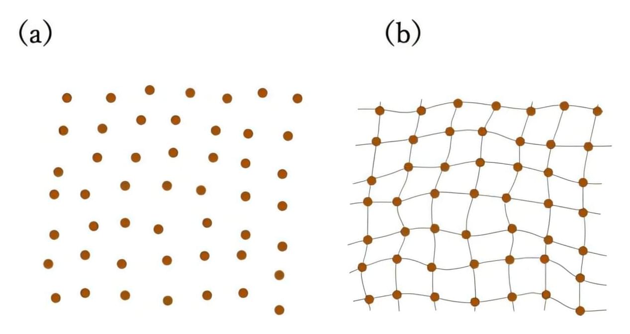
Most materials exist in an equilibrium state, meaning that the forces and torques on the material’s atoms are all balanced. Glasses, however, are a famous exception: they are amorphous solid materials whose atoms are always rearranging, albeit very slowly, toward an equilibrium state but do not exist in equilibrium.
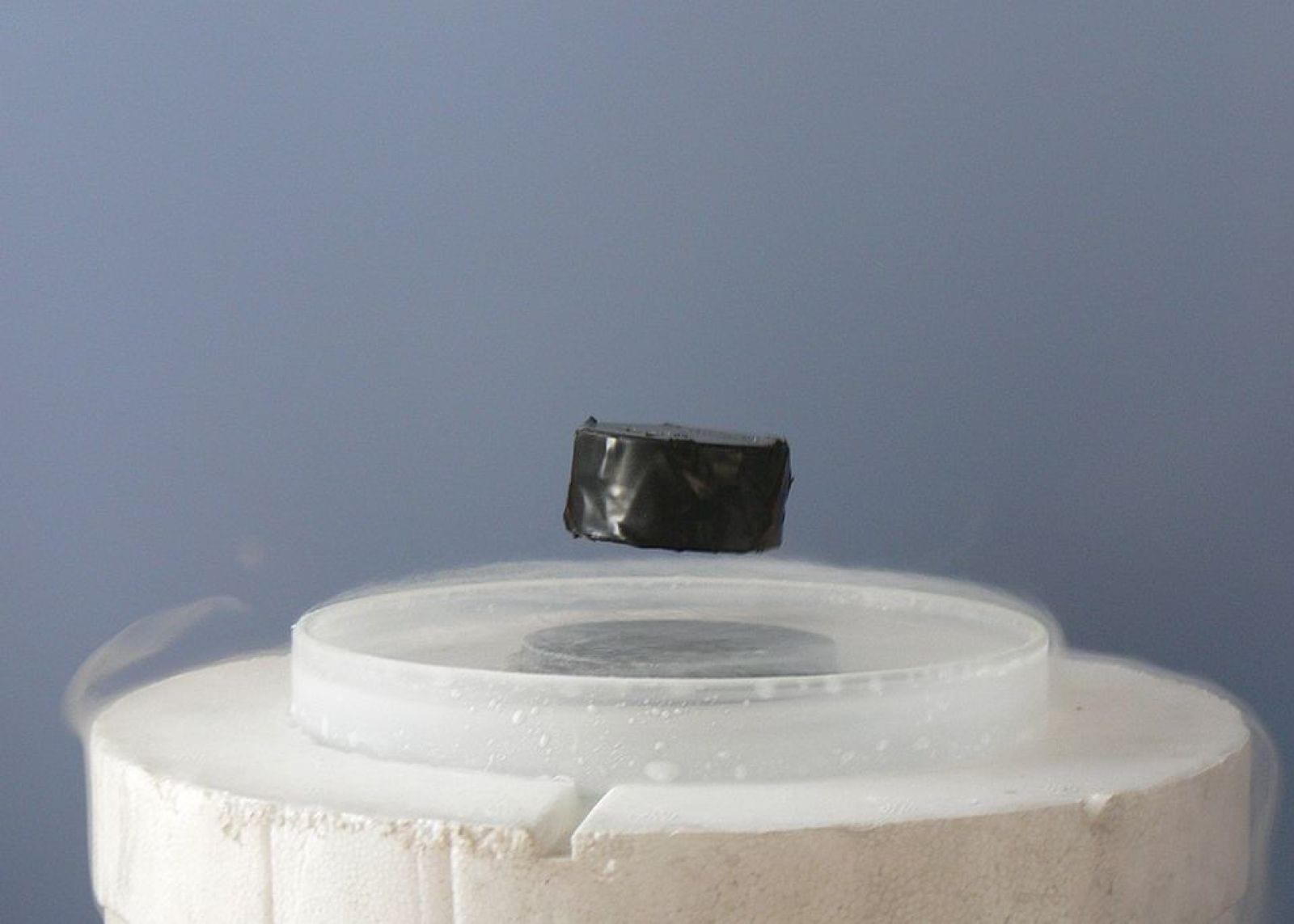
A team of scientists has succeeded in creating a copper-free superconducting material operating at record temperatures. This breakthrough could transform our approach to electronic and energy technologies.
Researchers at the National University of Singapore synthesized a copper-free superconducting oxide that operates at around 40 K (−233°C) under ambient pressure. This nickel-based material opens new perspectives for understanding high-temperature superconductivity. The results were published in Nature, marking a key milestone since the discovery of copper oxides in 1987.

IN A NUTSHELL 🌍 China’s dominance in gallium production is reshaping global semiconductor and battery industries. ⚠️ Japan has raised alarms about the strategic implications of China’s control over critical resources like gallium, germanium, and antimony. 🔗 The U.S. sanctions against China have intensified competition for strategic raw materials, leading to trade tensions. 🏭 The
The UMass Amherst-led team is challenging the common belief that perfect fillers are the best choice for creating thermally conductive polymers.
In the pursuit of developing next-generation materials for modern devices, materials that are lightweight, flexible, and highly efficient at dissipating heat, a research team led by the University of Massachusetts Amherst has uncovered a surprising insight: imperfection has its upsides.
Published in Science Advances.