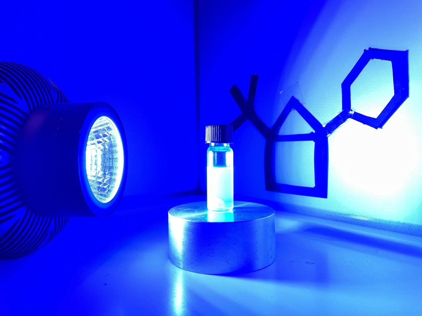
Menu

Blog

Archive for the ‘materials’ category: Page 28

Feb 4, 2024

Hexagonal copper disk lattice unleashes spin wave control

Posted by in categories: materials, robotics/AI

A collaborative group of researchers has potentially developed a means of controlling spin waves by creating a hexagonal pattern of copper disks on a magnetic insulator. The breakthrough is expected to lead to greater efficiency and miniaturization of communication devices in fields such as artificial intelligence and automation technology.

Details of the study were published in the journal Physical Review Applied on January 30, 2024.

In a magnetic material, the spins of electrons are aligned. When these spins undergo coordinated movement, they generate a kind of ripple in the magnetic order, dubbed . Spin waves generate little heat and offer an abundance of advantages for next-generation devices.

Feb 4, 2024

Hafnia Breakthrough Paves Way for Ultra-Fast, Efficient, Cheap Computer Memory

Posted by in categories: computing, materials

Scientists outline new processes for leveraging hafnia’s ferroelectric features with the aim of enhancing high-performance computing.

Scientists and engineers have been pushing for the past decade to leverage an elusive ferroelectric material called hafnium oxide, or hafnia, to usher in the next generation of computing memory. A team of researchers including the University of Rochester’s Sobhit Singh published a Proceedings of the National Academy of Sciences study outlining progress toward making bulk ferroelectric and antiferroelectric hafnia available for use in a variety of applications.

In a specific crystal phase, hafnia exhibits ferroelectric properties—that is, electric polarization that can be changed in one direction or another by applying an external electric field. This feature can be harnessed in data storage technology. When used in computing, ferroelectric memory has the benefit of non-volatility, meaning it retains its values even when powered off, one of several advantages over most types of memory used today.

Feb 3, 2024

How Invisible Light Is Shaping the Future of High-Speed Computing

Posted by in categories: computing, materials

New ultrafast method for controlling magnetic materials might enable next-generation information processing technologies.

As demands for computing resources continue to increase rapidly, scientists and engineers are looking for ways to build faster systems for processing information. One possible solution is to use patterns of electron spins, called spin waves, to transfer and process information much more rapidly than in conventional computers. So far, a major challenge has been in manipulating these ultrafast spin waves to do useful work.

Breakthrough in Spin Wave Manipulation.

Feb 3, 2024

New material design for transistors could downsize next-gen tech

Posted by in categories: computing, materials

By better taming the Jekyll-and-Hyde nature of an alternative to the semiconductor—one that transitions from electricity-resisting insulator to current-conducting metal—Nebraska’s Xia Hong and colleagues may have unlocked a new path to smaller, more efficient digital devices. The team reports its findings in the journal Nature Communications.

The semiconductor’s ability to conduct electricity in the Goldilocks zone—poorer than a metal, better than an insulator—positioned it as the just-right choice for engineers looking to build transistors, the tiny on-off switches that encode the 1s and 0s of binary. Apply some voltage to the control knob known as a gate insulator, and the semiconductor channel allows electric current to flow ; remove it, and that flow ceases.

Millions of those nanoscopic, semiconductor-based transistors now coat modern microchips, switching on and off to collectively process or store data. But as minuscule as the transistors already are, the demands of consumers and competition continue pushing to shrink them even further, either for the sake of squeezing in more functionality or downsizing the devices that house them.

Feb 3, 2024

Approaching the dream of the alchemist

Posted by in categories: innovation, materials

The EPFL team, using tellurite glass produced by their Tokyo Tech colleagues, applied their expertise in femtosecond laser technology to alter the glass and study the laser’s effect. After etching a simple line pattern onto a 1 cm diameter tellurite glass and exposing it to UV light and the visible spectrum, Torun found it could generate a current consistently for months.

Bellouard expressed his excitement at the breakthrough, saying, “We’re locally turning glass into a semiconductor using light. We’re essentially transforming materials into something else, perhaps approaching the dream of the alchemist!”

This development may pave the way for windows to function as single-material light-harvesting and sensing devices in the future.

Jan 31, 2024

MIT physicists turn pencil lead into “gold”

Posted by in categories: materials, physics

MIT physicists have metaphorically turned graphite, or pencil lead, into gold by isolating five ultrathin flakes stacked in a specific order. The resulting material can then be tuned to exhibit three important properties never before seen in natural graphite.

“It is kind of like one-stop shopping,” says Long Ju, an assistant professor in the Department of Physics and leader of the work, which is reported in the Oct. 5 issue of Nature Nanotechnology. “Nature has plenty of surprises. In this case, we never realized that all of these interesting things are embedded in graphite.”

Further, he says, “It is very rare material to find materials that can host this many properties.”

Jan 31, 2024

In a quantum coup, US finds first-ever 3D material that ‘locks’ electrons

Posted by in categories: materials, quantum physics

It was 1951 that a Japanese researcher found a two dimensional lattice structure that could lock electrons. It has taken over seven decades to find a 3D structure.

Jan 30, 2024

Researchers showcase new breakthroughs for unlocking the potential of plasmonics

Posted by in categories: materials, nanotechnology

Plasmonics are special optical phenomena that are understood as interactions between light and matter and possess diverse shapes, material compositions, and symmetry-related behavior. The design of such plasmonic structures at the nanoscale level can pave the way for optical materials that respond to the orientation of light (polarization), which is not easily achievable in bulk size and existing materials.

In this regard, “shadow growth” is a technique that utilizes vacuum deposition to produce nanoparticles from a wide range of 2D and 3D shapes at nanoscale. Recent research progress in controlling this shadow effect has broadened the possibilities for the creation of different nanostructures.

Now, in twin studies led by Assistant Professor Hyeon-Ho Jeong from the Gwangju Institute of Science and Technology (GIST), Republic of Korea, researchers have comprehensively shed light on the recent advances in shadow growth techniques for hybrid plasmonic nanomaterials, including clock-inspired designs containing magnesium (Mg).

Jan 30, 2024

Researchers slow down light in metasurfaces with record low loss

Posted by in categories: materials, nanotechnology

The speed of light can be intentionally reduced in various media. Various techniques have been developed over the years to slow down light, including electromagnetically induced transparency (EIT), Bose-Einstein condensate (BEC), photonic crystals, and stimulated Brillouin scattering (SBS).

Notably, researchers from Harvard, led by Lene Vestergaard Hau, reduced light speed to 17 m/s in an ultracold atomic gas using EIT, which sparked the interest in exploring EIT analogs in metasurfaces, a transformative platform in optics and photonics.

Despite the benefits, slow-light structures face a significant challenge: Loss, which limits storage time and interaction length. This issue is particularly severe for analogs of EIT due to scattering loss of nanoparticles and sometimes absorption loss of materials.

Jan 29, 2024

New biocompatible nanotweezers enhance control over diverse nanoparticles with versatility and precision

Posted by in categories: materials, nanotechnology

Highly adaptable optothermal nanotweezers leverage thermophoresis and thermo-osmosis to trap nanoparticles as small as 3.3 nm across materials without requiring surface modifications.

Page 28 of 274First2526272829303132Last