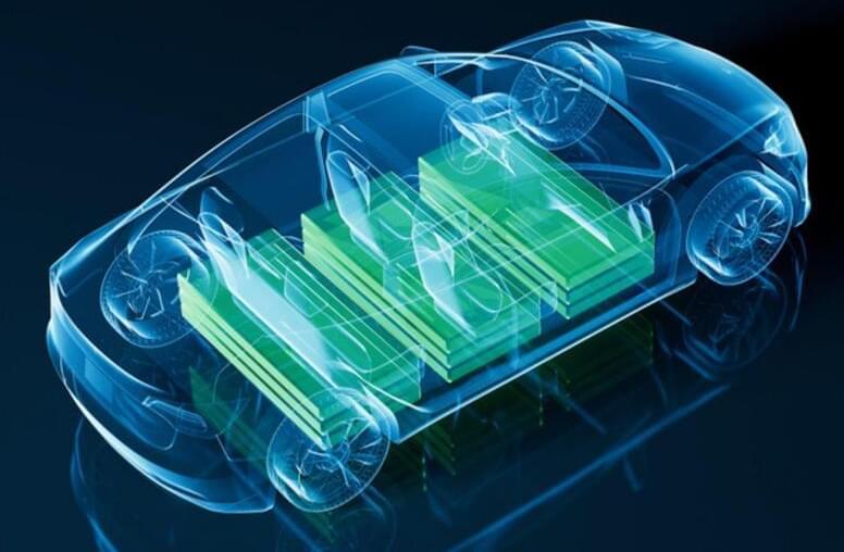
Scientists have yet to obtain a complete microscopic understanding of how a supercooled liquid behaves as it turns into a glass. Different theories can capture different aspects of the spatial and temporal dynamics of this process, but the assumptions behind these theories are, in some cases, mutually exclusive. Now Yoshihiko Nishikawa at Tohoku University, Japan, and Ludovic Berthier at the University of Montpellier, France, reconcile two competing descriptions of this glass-transition behavior using a recently developed lattice model [1].
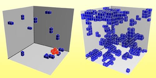
A prominent glass-transition theory known as random first-order transition theory holds that a cooling glass-forming liquid adopts a mosaic-like static structure with finite-range order. In this framework, so-called dynamic fluctuations—reorganizations of a material’s particles—occur when boundaries between mosaic “tiles” collectively rearrange. These fluctuations are fundamentally tied to static, region-to-region variations in a material’s structure. A competing theory known as dynamic-facilitation theory contains no assumptions about the system’s static structure or region-to-region variations. This theory postulates that dynamic fluctuations occur via local, small-scale particle rearrangements that trigger a reorganizational chain reaction that then propagates through the material.
For their study, Nishikawa and Berthier used a different theory to probe the glass transition of a supercooled liquid. Their three-dimensional lattice theory exhibits mosaic-like structural variations that are consistent with those from random first-order transition theory. However, the researchers found that the model’s predictions for the dynamic fluctuations more closely resemble those of the dynamic-facilitation framework. Nishikawa says that no current experiments can directly confirm the occurrence of these behaviors in real glass-forming materials. But he hopes to use the three-dimensional lattice model to reproduce some recently observed indirect experimental data.

