Metal organic frameworks (MOFs) on a bipyridinium basis can be excellent candidates to observe an ET due to their structural arrangement. Recently, Guo et al.12 reported a 2D semiconductor MOF composed by π-stacked redox active N-methylpyridinium cations, sandwiched by cyanide-bridged layers that shows light and temperature-induced color change with the formation of stable radicals even in an ambient atmosphere. In this case, the observed thermo-and photo-activated ET within these materials involves the pyridinium unit as acceptor and the uncoordinated CN- moiety as donor. These MOF structures are closely related to Prussian blue and/or Hofmann clathrate derivatives which offer excellent structural platforms to establish multifunctionality, due to their intrinsic magnetic properties: photomagnetism, magnetic ordering, valence tautomerism and/or a spin crossover (SCO)22,23,24,25,26.
In general, Hofmann clathrates are formed by three major building blocks, first off, aion metal center, second, a ligand (L) and lastly, a cyanometallate anion [M(CN)x]n– (x = 2 or 4, n = 1 or 2). Usually, this combination affords 2D planar metal−cyanide−metal sheets completed by a mono-or bidentate neutral organic ligand L, most often ammonia27, pyridine2830,31,32, triazole33,34,35,36,37 or pyrazine38,39,40 derivatives, with a general formula of {Fe(L)x[µ4-M’(CN)4]} (x = 1 or 2; M’= Ni, Pd or Pt) or {Fe(L)x[µ2-M(CN)2]} (x = 1 or 2; M= Cu, Ag or Au)28. The modulation of the ligand field around the iron center through the different units leads to the introduction of the SCO properties. To our knowledge, at least three exceptions to this general formula have been described in literature: i) if the ligand is a strong chelate, for example a quinoline derivative (aqin), 1D chains of [Fe(aqin)2(μ2-M(CN)4)] (M = NiII and PtII) are obtained, where [M(CN)4]2- acts as a bridge between the iron sites; ii) if the ligand is tetradentate, a {[Fe(μ4-bztpy)μ2-Pt(CN)4]·0.5bztpy} structure emerges, where 2D sheets, formed by the ligand and the FeII metal center, are again interconnected by [M(CN)4]2- building blocks42, and iii) very recently, Real et al. described two isomorphous structures, where the ligand carries a positive charge due to a spontaneous protonation during the crystallization process. The authors suggested that the positive charge could be responsible for an additional class of Hofmann-clathrates with the general formula {Fe(L)2[µ2-M(CN)4]}. It should be noted that in all of the above cases, the specific properties (electronic, steric, etc.) of the ligands are responsible for the final structure of these modified Hofmann-type clathrates, which, nevertheless, maintain a SCO behavior. Thus, we think that Hofmann-type clathrates offer an excellent structural platform to establish multifunctionality through introduction of a redox-active ligand, such as a bipyridinium-type derivative.
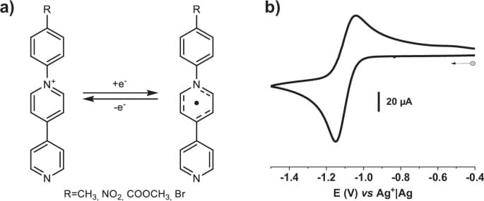
In this work, we explore this idea by synthesizing a large family of non-innocent ligands, which contain three functional building blocks (Fig. 1a; see Supplementary Figs 1 – 5 for characterization), the most important being a monocationic pyridinium unit that is responsible for the redox activity12,44,45,46,47. Attached to it, an aryl group allows for the fine-tuning of the delocalized electron density of the ligand by modifying the substituent R in para position. Lastly, a pyridine group is added to ensure the coordination to the iron center. The pyridinium moiety contains an electropositive, quaternary nitrogen atom that can be reduced to the highly air-sensitive neutral (radical) species (Fig. 1b). As demonstrated through several examples in the literature, the stability of the radical state can be largely improved by e.g. incorporating it in a MOF structure. In the case of the compound reported by Guo et al.12 the stabilization of the radical is due to π−π and cation-π interactions within the network. With this idea in mind, the abovementioned redox-active ligands were used to synthesize a family of Hofmann-type MOFs, which, as we show below, host a wealth of electronic phenomena, including both SCO and ET processes as well as redox activity…


