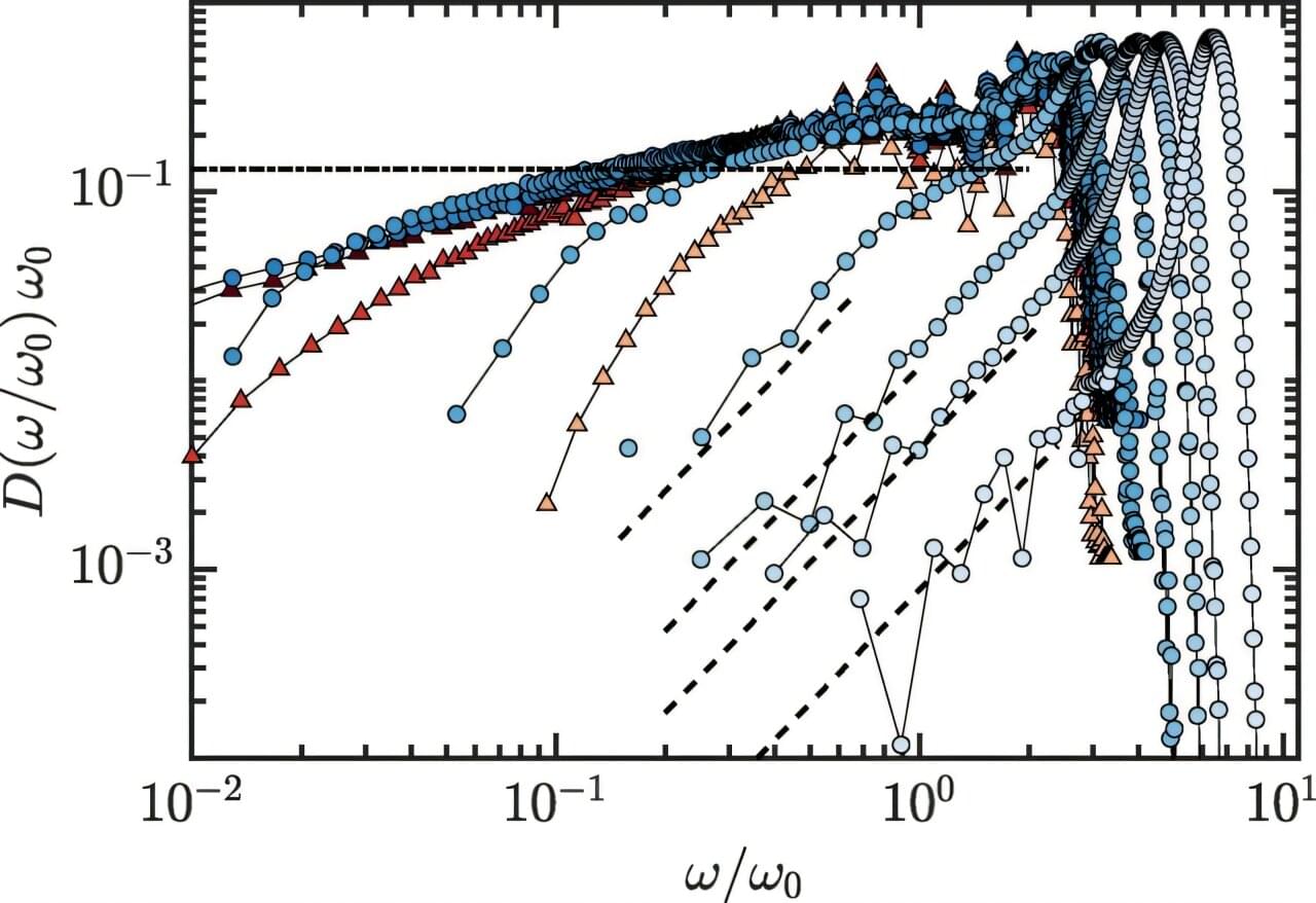
Menu

Blog

Archive for the ‘materials’ category: Page 108

Jun 22, 2021

MIT scientists made a shape-shifting material that morphs into a human face

Posted by in category: materials

New method based on double-curvature effect described by Gauss nearly 200 years ago.

Jun 21, 2021

Inventor creates new material that can keep buildings cool without air conditioning

Posted by in category: materials

I like this one, especially because using recycled materials has no loss in efficacy.


Beating the heat with paper.

Jun 20, 2021

Apollo Project for Water

Posted by in categories: materials, sustainability

With the drought in the west it is time to consider an Apollo Program to produce clean water. Breakthroughs in processing lithium and with graphene-based desalination membranes may point the way. (Meant to say almost 20 Million people — needed some coffee tonight!)

See the Special Deals at My Patriot Supply: www.PrepWithGreg.com.

Continue reading “Apollo Project for Water” »

Jun 17, 2021

Applied Materials: Wiring breakthrough will enable 3-nanometer chips

Posted by in categories: computing, materials

Applied Materials said it has reached a breakthrough in chip wiring that will enable semiconductor chip production to miniaturize to chips so the width between circuits can be as little as three billionths of a meter. Current chip factories are making 7nm and 5nm chips, so the 3nm chips represent the next generation of technology.

These 3nm production lines will be part of factories that cost more than $22 billion to build — and generate a lot more revenue than that. The breakthrough in chip wiring will enable logic chips to scale to three nanometers and beyond, the company said.

Chip manufacturing companies can use the wiring tools in their huge factories, and the transition from 5nm factories to 3nm factories could help ease a shortage of semiconductor chips that has plagued the entire electronics industry. But it will be a while before the chips go into production. In addition to interconnect scaling challenges, there are other issues related to the transistor (extending the use of FinFET transistors and transitioning to Gate All Around transistors), as well as patterning (extreme ultraviolet and multi-patterning).

Jun 17, 2021

Symmetry-enforced topological nodal planes at the Fermi surface of a chiral magnet

Posted by in categories: materials, transportation

Measurements on a chiral magnet show that non-symmorphic symmetries enforce topological crossings exactly at the Fermi level in certain materials; these crossings can be controlled by an applied magnetic field.

Jun 17, 2021

NASA Might Put a Huge Telescope on the Far Side of the Moon

Posted by in categories: cosmology, materials, robotics/AI

Observing the secrets of the universe’s “Dark Ages” will require capturing ultra-long radio wavelengths—and we can’t do that on Earth.


The universe is constantly beaming its history to us. For instance: Information about what happened long, long ago, contained in the long-length radio waves that are ubiquitous throughout the universe, likely hold the details about how the first stars and black holes were formed. There’s a problem, though. Because of our atmosphere and noisy radio signals generated by modern society, we can’t read them from Earth.

That’s why NASA is in the early stages of planning what it would take to build an automated research telescope on the far side of the moon. One of the most ambitious proposals would build the Lunar Crater Radio Telescope, the largest (by a lot) filled-aperture radio telescope dish in the universe. Another duo of projects, called FarSide and FarView, would connect a vast array of antennas—eventually over 100000, many built on the moon itself and made out of its surface material—to pick up the signals. The projects are all part of NASA’s Institute for Advanced Concepts (NIAC) program, which awards innovators and entrepreneurs with funding to advance radical ideas in hopes of creating breakthrough aerospace concepts. While they are still hypothetical, and years away from reality, the findings from these projects could reshape our cosmological model of the universe.

Continue reading “NASA Might Put a Huge Telescope on the Far Side of the Moon” »

Jun 16, 2021

Magnet Sets World Record at 45.5 Teslas

Posted by in category: materials

O,.o! Amazing 👏🙀😮


A new multicomponent, partially-superconducting electromagnet—currently the world’s strongest DC magnet of any kind—is poised to reveal a path to substantially stronger magnets still. The new magnet technology could help scientists study many other phenomena including nuclear fusion, exotic states of matter, “shape-shifting” molecules, and interplanetary rockets, to name a few.

The National High Magnetic Field Laboratory in Tallahassee, Florida is home to four types of advanced, ultra-strong magnets. One supports magnetic resonance studies. Another is configured for mass spectrometry. And a different type produces the strongest magnetic fields in the world. (Sister MagLab campuses at the University of Florida and Los Alamos National Laboratory provide three more high-capacity magnets for other fields of study.)

Continue reading “Magnet Sets World Record at 45.5 Teslas” »

Jun 15, 2021

New graphene display creates LEDs at an atomic level

Posted by in category: materials

Circa 2015 o,.o!


New graphene displays could pave the way for ultra-thin, incredibly durable, and highly efficient LCD technology — even at this early state of development.

Jun 15, 2021

Light-squashing spaceplates could lead to paper-thin smartphones

Posted by in categories: materials, mobile phones

Material layers compress empty space between optical components.

Jun 14, 2021

Israeli scientists show they can shrink optical technology by 1,000 times

Posted by in category: materials

Trapping and observing light in super-thin materials, Technion researchers say their work may pave way for new generation of tiny light-powered tech.