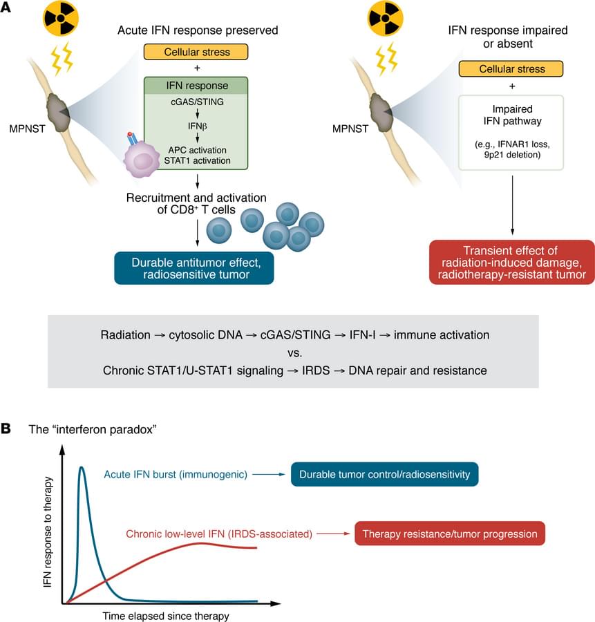
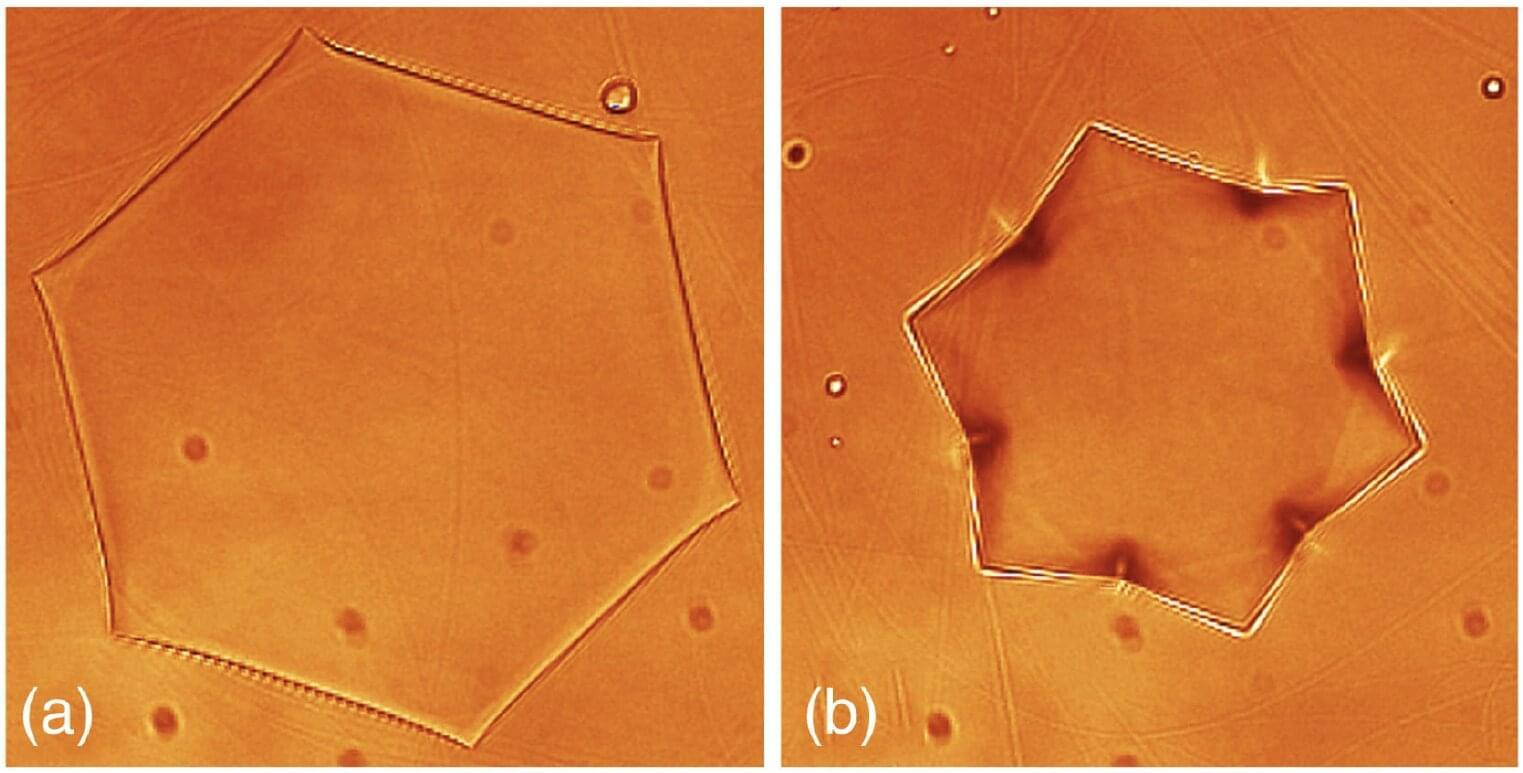
For the first time, researchers in France and Israel have observed how an emulsified liquid droplet can transform from a hexagon into a six-pointed star shape in response to rising temperature. Publishing their results in Physical Review Letters, a team led by Eli Sloutskin at Bar-Ilan University has shed new light on the mechanisms underlying this striking behavior, revealing a previously unseen form of “nano-origami,” that could inspire future generations of self-assembling nanostructures.
When tiny amounts of liquid are isolated, surface tension usually drives them to adopt a spherical shape—but over the past decade, researchers have uncovered far more complex behavior in emulsions of oil and water. In these systems, droplets are stabilized by surfactant molecules, which reduce the surface tension between the two liquids.
Under carefully controlled temperature changes, these droplets can undergo dramatic shape transformations. Previous studies have shown spheres turning into icosahedra, and then flattening into triangular, parallelogram or hexagonal, lens-like shapes with exclusively convex edges.


