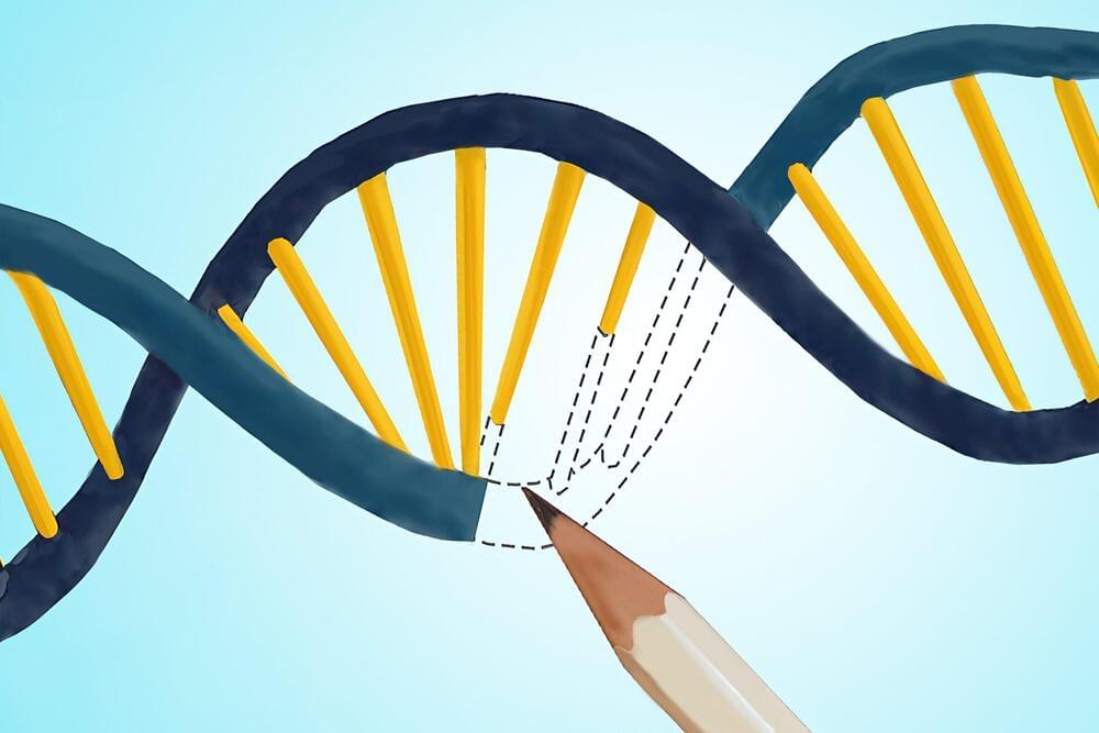
Through years of engineering gene-editing systems, researchers have developed a suite of tools that enable the modification of genomes in living cells, akin to “genome surgery.” These tools, including ones based on a natural system known as CRISPR/Cas9, offer enormous potential for addressing unmet clinical needs, underscored by the recent FDA approval of the first CRISPR/Cas9-based therapy.
A relatively new approach called “prime editing” enables gene-editing with exceptional accuracy and high versatility, but has a critical tradeoff: variable and often low efficiency of edit installation. In other words, while prime edits can be made with high precision and few unwanted byproducts, the approach also often fails to make those edits at reasonable frequencies.
In a paper that appeared in print in the journal Nature on April 18, 2024, Princeton scientists Jun Yan and Britt Adamson, along with several colleagues, describe a more efficient prime editor.
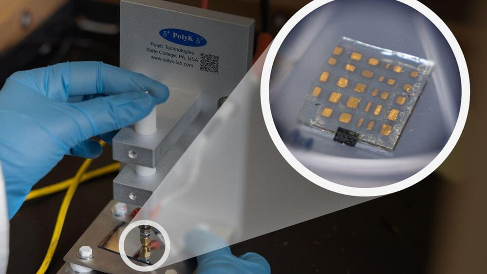
Dielectric capacitors are ubiquitous components that play a vital role in electronic devices and energy storage systems. Their ability to rapidly discharge significant amounts of energy makes them indispensable for high-power applications.
“High-energy and high-power capacitors are the backbone of reliable power supplies, especially as we transition towards renewable energy sources,” explains Alamgir Karim, Dow Chair and Welch Foundation Professor of Chemical Engineering at UH and a faculty mentor on the project. “However, current dielectric capacitors fall short in terms of energy storage capacity compared to other options like batteries. The advantage of capacitors lies in their superior power density, making them a more suitable choice for various applications.”
The key factor influencing a capacitor’s energy storage is a combination of its permittivity (ε) and dielectric breakdown strength (EBD). Professor Karim emphasizes, “To enhance a capacitor’s energy storage, advancements in both these aspects are crucial.”
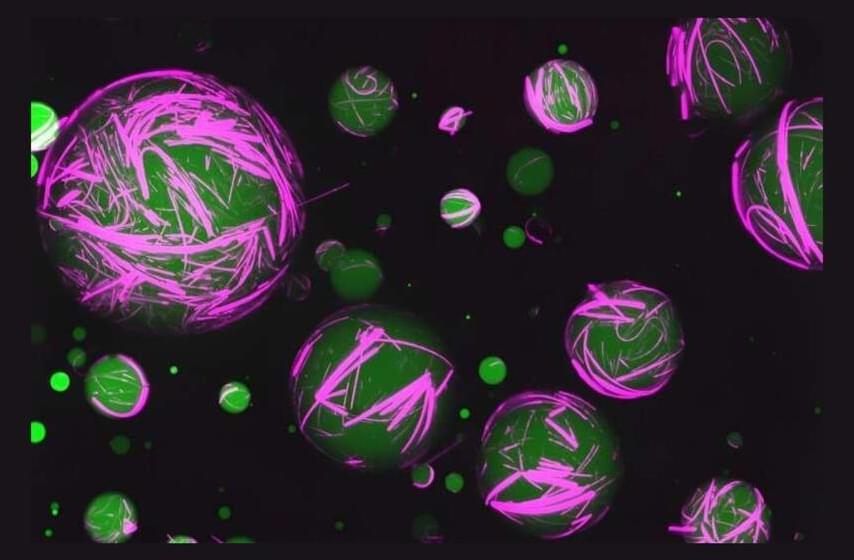
Instead of creating materials that are made to last, Freeman says their materials are made to task — perform a specific function and then modify themselves to serve a new function.
This achievement holds significant promise for advancements in regenerative medicine, drug delivery methods, and diagnostic technologies.
“With this discovery, we can think of engineering fabrics or tissues that can be sensitive to changes in their environment and behave in dynamic ways,” states Freeman.
In order to terraform new planets, we will need to be able transport entire ecologies & ecosystems through interstellar space in the future. Today we will examine how we could build and maintain such environments inside vast arks, generations ships able to colonize our galaxy, and the challenges these starships will face maintaining not just stores of DNA and genetic material but living organisms which depend heavily on other members of their species and other species to survive and thrive, not least of which is human ourselves. Visit our sponsor, Brilliant: https://brilliant.org/IsaacArthur/ Join this channel to get access to perks: / @isaacarthursfia Visit our Website: http://www.isaacarthur.net Join Nebula: https://go.nebula.tv/isaacarthur Support us on Patreon: / isaacarthur Support us on Subscribestar: https://www.subscribestar.com/isaac-a… Group: / 1,583,992,725,237,264 Reddit: / isaacarthur Twitter: / isaac_a_arthur on Twitter and RT our future content. SFIA Discord Server: / discord Listen or Download the audio of this episode from Soundcloud: Episode’s Audio-only version: / exporting-earth Episode’s Narration-only version: / exporting-earth-ships-narration-only Credits: Exporting Earth Episode 150, Season 4 E36 Writers: Isaac Arthur Editors: Darius Said Gregory Leal https://www.gregschool.org/ Jerry Guern Konstantin Sokerin Laura Graham Mark Warburton Matthew Acker Sigmund Kopperud Stuart Graham https://beyondnerva.wordpress.com Producer: Isaac Arthur Cover Artist: Jakub Grygier https://www.artstation.com/jakub_grygier Graphics Team: Darth Biomech https://www.artstation.com/darth_biomech Fishy Tree https://www.deviantart.com/fishytree/ Jarred Eagley Jeremy Jozwik https://www.artstation.com/zeuxis_of_… Katie Byrne Ken York / ydvisual Krisitijan Tavcar https://www.miragedereve.com LegionTech Studios Sam McNamara Sergio Boterio https://www.artstation.com/sboterod?f… Narrator: Isaac Arthur Music Manager: Luca DeRosa — [email protected] Music: Dracovallis, “Golden Meadows” https://dracovallis.bandcamp.com/ NJ Mandaville, “Intrumental Background 1” / nj-mandaville Kevin Macleod, “Infinite Wonder” / @incompetech_kmac Chris Zabriskie, “Candlepower” http://chriszabriskie.com Kai Engel, “Endless Story About Sun and Moon” https://www.kai-engel.com/ Lombus, “Amino” https://lombus.bandcamp.com Aerium, “Windmill Forests” / @officialaerium Epic Mountain, “Rising Sky” / epicmountain.
How can we guarantee that data sent over the internet is only accessible to its intended recipient? Currently, our data is secured using encryption methods based on the premise that factoring large numbers is a complex task. However, as quantum computing advances, these encryption techniques may become vulnerable and potentially ineffective in the future.
Encryption by means of physical laws
Tobias Vogl, a professor of Quantum Communication Systems Engineering, is working on an encryption process that relies on principles of physics. “Security will be based on the information being encoded into individual light particles and then transmitted. The laws of physics do not permit this information to be extracted or copied. When the information is intercepted, the light particles change their characteristics. Because we can measure these state changes, any attempt to intercept the transmitted data will be recognized immediately, regardless of future advances in technology,” says Tobias Vogl.
The galaxy is a vast place with billions of potential new worlds for humanity to colonize, but interstellar space is so enormous that reaching even the nearest stars and planets by spaceship would take decades at best, and maybe many centuries. Even on arrival terraforming those barren planets would take just as long.
Two options for overcoming the immensity of space and time are the Seed Ship and the Data Ship, automated vessels able to colonize the worlds for us. We will examine those today, their advantages, limitations, and misconceptions, and variations of them we might use to seed the stars. Join this channel to get access to perks: / @isaacarthursfia. Visit our Website: http://www.isaacarthur.net. Join Nebula: https://go.nebula.tv/isaacarthur. Support us on Patreon: / isaacarthur. Support us on Subscribestar: https://www.subscribestar.com/isaac-a… Group: / 1,583,992,725,237,264 Reddit: / isaacarthur Twitter: / isaac_a_arthur on Twitter and RT our future content. SFIA Discord Server: / discord Listen or Download the audio of this episode from Soundcloud: Episode’s Audio-only version: / seeding-the-stars Episode’s Narration-only version: / seeding-the-stars-narration-only Credits: Seeding the Stars Episode 166, Season 4 E52 Writers: Isaac Arthur Editors: Alex Chamak A.T. Long Cooper de Ruiter D. Hemanshi Daniel McNamara Darius Said Edward Nardella Evan Schultheis Keith Blockus Mark Warburton Matthew Acker Safia Postgate Stuart Graham https://beyondnerva.wordpress.com Sigmund Kopperud Producer: Isaac Arthur Cover Artist: Jakub Grygier https://www.artstation.com/jakub_grygier Graphics Team: Bryan Versteeg http://spacehabs.com Darth Biomech https://www.artstation.com/darth_biomech Fishy Tree https://www.deviantart.com/fishytree/ Jarred Eagley Jeremy Jozwik https://www.artstation.com/zeuxis_of_… Justin Dixon LegionTech Studios Mihail Yordanov Sam McNamara Serigio Botero https://www.artstation.com/sboterod?f… SpaceResourcesCGI Audio Editing Eric Schneider Narrator: Isaac Arthur Music Manager: Luca DeRosa — [email protected] Music: Markus Junnikkala, “Plotting a Course” https://www.markusjunnikkala.com/ Paradox Interactive, Andreas Waldetoft, “Dark Minds” https://www.paradoxplaza.com Lombus, “Hydrogen Sonata” https://lombus.bandcamp.com Paradox Interactive, “In Search of Life” https://www.paradoxplaza.com Serena Elis, “Between the Space” / serenaelis Taras Harkavyi, “Alpha-and-…” https://www.discogs.com/artist/625697… Paradox Interactive, Andreas Waldetoft, “The Birth of a Star” https://www.paradoxplaza.com Ayreon, “The Theory of Everything, Part 1″ / @arjenalucassen. Facebook Group: / 1583992725237264 Reddit: / isaacarthur. Twitter: / isaac_a_arthur on Twitter and RT our future content. SFIA Discord Server: / discord.
Listen or Download the audio of this episode from Soundcloud: Episode’s Audio-only version: / seeding-the-stars. Episode’s Narration-only version: / seeding-the-stars-narration-only.
Credits: Seeding the Stars. Episode 166, Season 4 E52
A team at Texas A&M University is taking significant steps for the development of a new generation of energy storage devices. They aim to develop a device that can combine the benefits of current technologies while addressing their limitations.
Dr. Abdoulaye Djire, a chemical engineering professor at Texas A&M University, as well as a few chemistry engineering graduates are focusing on MXenes, which is expected to be a compelling alternative to conventional lithium-ion batteries. Currently, the team is exploring the major advantages of nitride MXenes.
Granular materials, those made up of individual pieces, whether grains of sand or coffee beans or pebbles, are the most abundant form of solid matter on Earth. The way these materials move and react to external forces can determine when landslides or earthquakes happen, as well as more mundane events such as how cereal gets clogged coming out of the box.
Yet, analyzing the way these flow events take place and what determines their outcomes has been a real challenge, and most research has been confined to two-dimensional experiments that don’t reveal the full picture of how these materials behave.
Now, researchers at MIT have developed a method that allows for detailed 3D experiments that can reveal exactly how forces are transmitted through granular materials, and how the shapes of the grains can dramatically change the outcomes. The new work may lead to better ways of understanding how landslides are triggered, as well as how to control the flow of granular materials in industrial processes. The findings are described in the journal PNAS in a paper by MIT professor of civil and environmental engineering Ruben Juanes and Wei Li SM ’14, PhD ’19, who is now on the faculty at Stony Brook University.
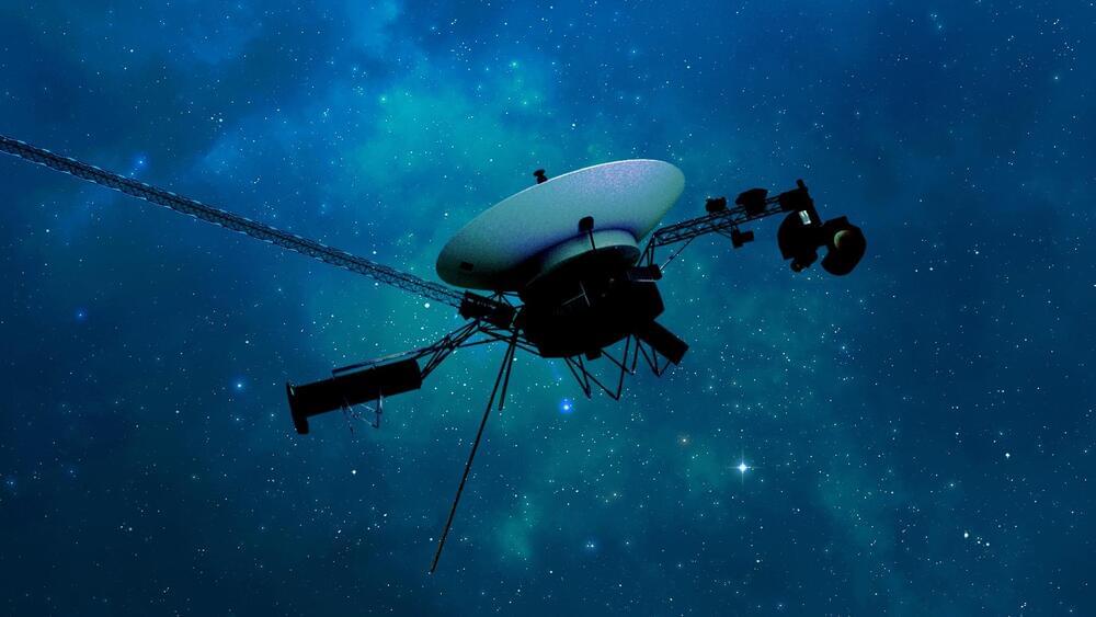
After some inventive sleuthing, the mission team can — for the first time in five months — check the health and status of the most distant human-made object in existence.
Observations of the Southern Ocean show that wind can produce the surface states needed to generate rare “rogue” waves.
Researchers still disagree on what causes rare and large “rogue waves,” which can damage ships, lighthouses, and other structures. Now, using combined measurements of wave heights and wind speed in an oceanic region known for its rough seas, a research team has demonstrated that wind can produce the wave conditions expected to lead to rogue waves [1]. Previously, this idea was demonstrated only in laboratory experiments. The researchers hope this new understanding will contribute to the development of methods for predicting this dangerous phenomenon.
There is no consensus on what causes rogue waves in the ocean, says Alessandro Toffoli, an expert in infrastructure engineering at the University of Melbourne, Australia. One prominent view is that oceanic rogue waves occur purely through a statistical effect: although waves typically follow a “normal,” or Gaussian, distribution, with heights strongly clustering around an average, a fortuitous convergence of many such waves can occasionally produce a very large wave.