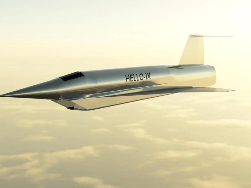
Toggle light / dark theme

The startup is hiring Ritesh Jain, VP of engineering at Intel, to help it move from the prototype phase of its chip development to mass production.


ESA is prepping to send a spacecraft to Venus — a feat which will require state-of-the-art methods to get through the planet’s grueling atmosphere.

The subtractive manufacturing process involves etching, drilling, or cutting from a solid board to build the final product. It is ideal for applications using a wide variety of materials and in the PCB fabrication of large-size products. In the additive manufacturing process, a product is developed by adding material one layer at a time and bonding the layers together until the final product is ready. The ability to control material density and the possibility of including intricate features makes this process versatile. It is used in a range of engineering and manufacturing applications, especially in custom manufacturing.

Benefits of 3D printing in medical device manufacturing.

3D printing is economical and offers quick PCB prototyping without the need for complex manufacturing steps. It optimizes the PCB design process by avoiding possible design faults in the initial PCB design stages. 3D printing is easy on flex PCBs and multilayer PCB printing is possible using the latest design software. With the growing manufacturing trends and improving software, 3D printing will be more than a prototyping tool and can be a viable alternative for production parts. 3D printing has been recently used for the end-part manufacturing of several medical devices like hearing aids, dental implants, and more. It is more beneficial for low-volume productions.

Circa 2013 😃


News: the world’s first building to be powered entirely by algae is being piloted in Hamburg, Germany, by engineering firm Arup.

The “bio-adaptive facade”, which Arup says is the first of its kind, uses live microalgae growing in glass louvres to generate renewable energy and provide shade at the same time.

Installed in the BIQ building as part of the International Building Exhibition, the algae are continuously supplied with liquid nutrients and carbon dioxide via a water circuit running through the facade.

Quantum entanglement is one of the most fundamental and intriguing phenomena in nature. Recent research on entanglement has proven to be a valuable resource for quantum communication and information processing. Now, scientists from Japan have discovered a stable quantum entangled state of two protons on a silicon surface, opening doors to an organic union of classical and quantum computing platforms and potentially strengthening the future of quantum technology.

One of the most interesting phenomena in quantum mechanics is “quantum entanglement.” This phenomenon describes how certain particles are inextricably linked, such that their states can only be described with reference to each other. This particle interaction also forms the basis of quantum computing. And this is why, in recent years, physicists have looked for techniques to generate entanglement. However, these techniques confront a number of engineering hurdles, including limitations in creating large number of “qubits” (quantum bits, the basic unit of quantum information), the need to maintain extremely low temperatures (1 K), and the use of ultrapure materials. Surfaces or interfaces are crucial in the formation of quantum entanglement. Unfortunately, electrons confined to surfaces are prone to “decoherence,” a condition in which there is no defined phase relationship between the two distinct states.

A novel bioremediation technology for cleaning up per-and polyfluoroalkyl substances, or PFAS, chemical pollutants that threaten human health and ecosystem sustainability, has been developed by Texas A&M AgriLife researchers. The material has potential for commercial application for disposing of PFAS, also known as “forever chemicals.”

Published July 28 in Nature Communications, the was a collaboration of Susie Dai, Ph.D., associate professor in the Texas A&M Department of Plant Pathology and Microbiology, and Joshua Yuan, Ph.D., chair and professor in Washington University in St. Louis Department of Energy, Environmental and Chemical Engineering, formerly with the Texas A&M Department of Plant Pathology and Microbiology.

Removing PFAS contamination is a challenge

PFAS are used in many applications such as food wrappers and packaging, dental floss, fire-fighting foam, nonstick cookware, textiles and electronics. These days, PFAS are widely distributed in the environment from manufacturing or from products containing the chemicals, said Dai.

A team of researchers from the National University of Singapore (NUS) has developed a novel technique that allows Physically Unclonable Functions (PUFs) to produce more secure, unique ‘fingerprint’ outputs at a very low cost. This achievement enhances the level of hardware security even in low-end systems on chips.

Traditionally, PUFs are embedded in several commercial chips to uniquely distinguish one from another by generating a secret key, similar to an individual fingerprint. Such a technology prevents hardware piracy, chip counterfeiting and physical attacks.

The research team from the Department of Electrical and Computer Engineering at the NUS Faculty of Engineering has taken silicon chip fingerprinting to the next level with two significant improvements: firstly, making PUFs self-healing; and secondly, enabling them to self-conceal.

Perovskite solar cells (PSCs) are promising solar technologies. Although low-cost wet processing has shown advantages in small-area PSC fabrication, the preparation of uniform charge transport layers with thickness of several nanometers from solution for meter-sized large area products is still challenging.

Recently, a research group led by Prof. LIU Shengzhong from the Dalian Institute of Chemical Physics (DICP) of the Chinese Academy of Sciences (CAS) has developed a facile surface redox engineering (SRE) strategy for vacuum-deposited NiO x to match the slot-die-coated perovskite, and fabricated high-performance large-area perovskite submodules.

This work was published in Joule (“Surface redox engineering of vacuum-deposited NiO x for top-performance perovskite solar cells and modules”).

Researchers from MIT

MIT is an acronym for the Massachusetts Institute of Technology. It is a prestigious private research university in Cambridge, Massachusetts that was founded in 1861. It is organized into five Schools: architecture and planning; engineering; humanities, arts, and social sciences; management; and science. MIT’s impact includes many scientific breakthroughs and technological advances. Their stated goal is to make a better world through education, research, and innovation.

Microplastics, tiny particles of plastic that are now found worldwide in the air, water, and soil, are increasingly recognized as a serious pollution threat, and have been found in the bloodstream of animals and people around the world.

Some of these microplastics are intentionally added to a variety of products, including agricultural chemicals, paints, cosmetics, and detergents—amounting to an estimated 50,000 tons a year in the European Union alone, according to the European Chemicals Agency. The EU has already declared that these added, nonbiodegradable microplastics must be eliminated by 2025, so the search is on for suitable replacements, which do not currently exist.

Now, a team of scientists at MIT and elsewhere has developed a system based on silk that could provide an inexpensive and easily manufactured substitute. The new process is described in a paper in the journal Small, written by MIT postdoc Muchun Liu, MIT professor of civil and environmental engineering Benedetto Marelli, and five others at the chemical company BASF in Germany and the U.S.