La Intel Xe-HPG cada vez es más real y después de varios rumores se han podido ver las primeras imágenes de esta GPU gaming.

In January 2020 we released the fly “hemibrain” connectome — an online database providing the morphological structure and synaptic connectivity of roughly half of the brain of a fruit fly (Drosophila melanogaster). This database and its supporting visualization has reframed the way that neural circuits are studied and understood in the fly brain. While the fruit fly brain is small enough to attain a relatively complete map using modern mapping techniques, the insights gained are, at best, only partially informative to understanding the most interesting object in neuroscience — the human brain.
Today, in collaboration with the Lichtman Laboratory at Harvard University, we are releasing the “H01” dataset, a 1.4 petabyte rendering of a small sample of human brain tissue, along with a companion paper, “A connectomic study of a petascale fragment of human cerebral cortex.” The H01 sample was imaged at 4nm-resolution by serial section electron microscopy, reconstructed and annotated by automated computational techniques, and analyzed for preliminary insights into the structure of the human cortex. The dataset comprises imaging data that covers roughly one cubic millimeter of brain tissue, and includes tens of thousands of reconstructed neurons, millions of neuron fragments, 130 million annotated synapses, 104 proofread cells, and many additional subcellular annotations and structures — all easily accessible with the Neuroglancer browser interface.
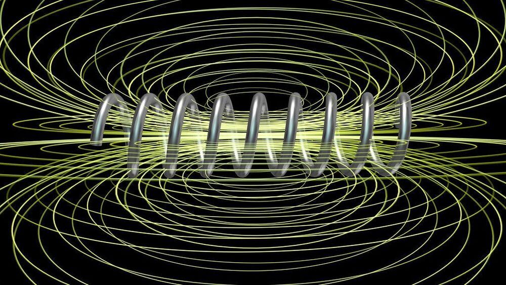
Physicists at the University of Bath in the UK, in collaboration with researchers from the USA, have uncovered a new mechanism for enabling magnetism and superconductivity to co-exist in the same material. Until now, scientists could only guess how this unusual coexistence might be possible. The discovery could lead to applications in green energy technologies and in the development of superconducting devices, such as next-generation computer hardware.
As a rule, superconductivity (the ability of a material to pass an electrical current with perfect efficiency) and magnetism (seen at work in fridge magnets) make poor bedfellows because the alignment of the tiny electronic magnetic particles in ferromagnets generally leads to the destruction of the electron pairs responsible for superconductivity. Despite this, the Bath researchers have found that the iron-based superconductor RbEuFe4As4, which is superconducting below-236°C, exhibits both superconductivity and magnetism below-258°C.
Physics postgraduate research student David Collomb, who led the research, explained: There’s a state in some materials where, if you get them really cold—significantly colder than the Antarctic—they become superconducting. But for this superconductivity to be taken to next-level applications, the material needs to show co-existence with magnetic properties. This would allow us to develop devices operating on a magnetic principle, such as magnetic memory and computation using magnetic materials, to also enjoy the benefits of superconductivity.
Batteries and fuel cells often rely on a process known as ion diffusion to function. In ion diffusion, ionized atoms move through solid materials, similar to the process of water being absorbed by rice when cooked. Just like cooking rice, ion diffusion is incredibly temperature-dependent and requires high temperatures to happen fast.
This temperature dependence can be limiting, as the materials used in some systems like fuel cells need to withstand high temperatures sometimes in excess of 1000 degrees Celsius. In a new study, a team of researchers at MIT and the University of Muenster in Germany showed a new effect, where ion diffusion is enhanced while the material remains cold, by only exciting a select number of vibrations known as phonons. This new approach—which the team refers to as “phonon catalysis”—could lead to an entirely new field of research. Their work was published in Cell Reports Physical Science.
In the study, the research team used a computational model to determine which vibrations actually caused ions to move during ion diffusion. Rather than increasing the temperature of the entire material, they increased the temperature of just those specific vibrations in a process they refer to as targeted phonon excitation.

JÜLICH, Germany, May 28, 2021 — Quantum systems are considered extremely fragile. Even the smallest interactions with the environment can result in the loss of sensitive quantum effects. In the renowned journal Science, however, researchers from TU Delft, RWTH Aachen University and Forschungszentrum Jülich now present an experiment in which a quantum system consisting of two coupled atoms behaves surprisingly stable under electron bombardment. The experiment provide an indication that special quantum states might be realised in a quantum computer more easily than previously thought.
 The so-called decoherence is one of the greatest enemies of the quantum physicist. Experts understand by this the decay of quantum states. This inevitably occurs when the system interacts with its environment. In the macroscopic world, this exchange is unavoidable, which is why quantum effects rarely occur in daily life. The quantum systems used in research, such as individual atoms, electrons or photons, are better shielded, but are fundamentally similarly sensitive.
“Systems subject to quantum physics, unlike classical objects, are not sharply defined in all their properties. Instead, they can occupy several states at once. This is called superposition,” Markus Ternes explains. “A famous example is Schrödinger’s thought experiment with the cat, which is temporarily dead and alive at the same time. However, the superposition breaks down as soon as the system is disturbed or measured. What is left then is only a single state, which is the measured value,” says the quantum physicist from Forschungszentrum Jülich and RWTH Aachen University.

Harvard University researchers have made a breakthrough in battery tech: a long-lasting solid-state lithium battery.
“A lithium-metal battery is considered the holy grail for battery chemistry,” researcher Xin Li told the Harvard Gazette.
Strong, cheaper, faster: Most of today’s electric vehicles (EVs) are powered by lithium-ion batteries, the same type of battery you’ll find in your laptop or smartphone.
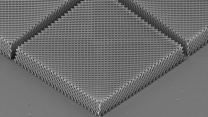
Scientists have taken a step towards the creation of powerful devices that harness magnetic charge by creating the first ever three-dimensional replica of a material known as a spin-ice.
Spin ice materials are extremely unusual as they possess so-called defects which behave as the single pole of a magnet.
These single pole magnets, also known as magnetic monopoles, do not exist in nature; when every magnetic material is cut into two it will always create a new magnet with a north and south pole.
More on thymus regeneration. Unless I understood wrong one patient’s epigenetic clock went from his mid 50’s to early 40’s.
Foresight Biotech & Health Extension Meeting sponsored by 100 Plus Capital.
2021 program & apply to join: https://foresight.org/biotech-health-extension-program/
Greg Fahy, Intervene Immune.
Thymus Rejuvenation Progress Update.
- Designed and led the TRIIM trial; Published the first report of thymus regeneration in a normal human; Granted patents on methods for and applications of human thymus regeneration.

## SCIENCE ADVANCES • MAY 24, 2021 # *by Vienna University of Technology*
In everyday life, phase transitions usually have to do with temperature changes–for example, when an ice cube gets warmer and melts. But there are also different kinds of phase transitions, depending on other parameters such as magnetic field. In order to understand the quantum properties of materials, phase transitions are particularly interesting when they occur directly at the absolute zero point of temperature. These transitions are called “quantum phase transitions” or a “quantum critical points.”
Such a quantum critical point has now been discovered by an Austrian-American research team in a novel material, and in an unusually pristine form. The properties of this material are now being further investigated.
It is suspected that the material could be a so-called Weyl-Kondo semimetal, which is considered to have great potential for quantum technology due to special quantum states (so-called topological states). If this proves to be true, a key for the targeted development of topological quantum materials would have been found.
This surprising result is probably related to the fact that the behavior of electrons in this material has some special features. “It is a highly correlated electron system. This means that the electrons interact strongly with each other, and that you cannot explain their behavior by looking at the electrons individually.
If there are only relatively few free electrons, as is the case in a semimetal, then the Kondo effect is unstable. This could be the reason for the quantum critical behavior of the material: the system fluctuates between a state with and a state without the Kondo effect, and this has the effect of a phase transition at zero temperature.
**Quantum fluctuations could lead to Weyl particles**