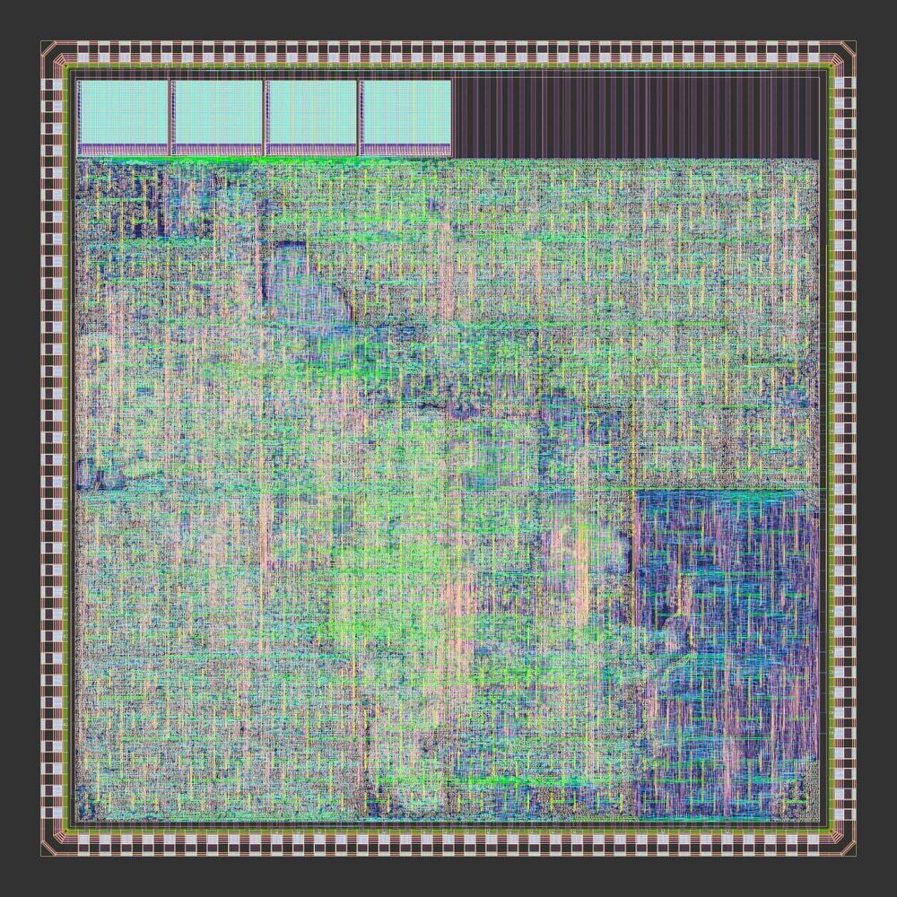
Manufactured on tsmc’s 180 nm process.
Libre-SOC developers sent the first test ASIC to TSMC’s manufacturing facilities.

Infinity Cache is one of the headline features found in AMD’s RDNA 2 – the GPU architecture behind the next generation of gaming graphics, including the PS5, the Xbox Series X and, of course, AMD’s own Radeon RX 6000 graphics cards. But, what is Infinity Cache?
Read on to learn more about Infinity Cache, how it works and where you can find it.
Infinity Cache is an all-new cache level AMD says will improve the efficiency and performance of its RDNA 2 architecture during 4K and 1440p gaming.

Early in its history, computing was dominated by time-sharing systems. These systems were powerful machines (for their time, at least) that multiple users connected to in order to perform computing tasks. To an extent, quantum computing has repeated this history, with companies like Honeywell, IBM, and Rigetti making their machines available to users via cloud services. Companies pay based on the amount of time they spend executing algorithms on the hardware.
For the most part, time-sharing works out well, saving companies the expenses involved in maintaining the machine and its associated hardware, which often includes a system that chills the processor down to nearly absolute zero. But there are several customers—companies developing support hardware, academic researchers, etc.—for whom access to the actual hardware could be essential.
The fact that companies aren’t shipping out processors suggests that the market isn’t big enough to make production worthwhile. But a startup from the Netherlands is betting that the size of the market is about to change. On Monday, a company called QuantWare announced that it will start selling quantum processors based on transmons, superconducting loops of wire that form the basis of similar machines used by Google, IBM, and Rigetti.


A team of researchers affiliated with multiple institutions in China, working at the University of Science and Technology of China, has achieved another milestone in the development of a usable quantum computer. The group has written a paper describing its latest efforts and have uploaded it to the arXiv preprint server.
Back in 2019, a team at Google announced that they had achieved “quantum supremacy” with their Sycamore machine—a 54 qubit processor that carried out a calculation that would have taken a traditional computer approximately 10000 years to complete. But that achievement was soon surpassed by other teams from Honeywell and a team in China. The team in China used a different technique, one that involved the use of photonic qubits—but it was also a one-trick pony. In this new effort, the new team in China, which has been led by Jian-Wei Pan, who also led the prior team at the University of Science and Technology has achieved another milestone.
The new effort was conducted with a 2D programable computer called Zuchongzhi—one equipped to run with 66 qubits. In their demonstration, the researchers used only 56 of those qubits to tackle a well-known computer problem—sampling the output distribution of random quantum circuits. The task requires a variety of computer abilities that involve mathematical analysis, matrix theory, the complexity of certain computations and probability theory—a task approximately 100 times more challenging than the one carried out by Sycamore just two years ago. Prior research has suggested the task set before the Chinese machine would take a conventional computer approximately eight years to complete. Zuchongzhi completed the task in less than an hour and a half. The achievement by the team showed that the Zuchongzhi machine is capable of tackling more than just one kind of task.

In 2015, after 85 years of searching, researchers confirmed the existence of a massless particle called the Weyl fermion. With the unique ability to behave as both matter and anti-matter inside a crystal, this quasiparticle is like an electron with no mass. The story begun in 1928 when Dirac proposed an equation for the foundational unification of quantum mechanics and special relativity in describing the nature of the electron. This new equation suggested three distinct forms of relativistic particles: the Dirac, the Majorana, and the Weyl fermions. And recently, an analog of Weyl fermions has been discovered in certain electronic materials exhibiting a strong spin orbit coupling and topological behavior. Just as Dirac fermions emerge as signatures of topological insulators, in certain types of semimetals, electrons can behave like Weyl fermions.
These Weyl fermions are what can be called quasiparticles, which means they can only exist in a solid such as a crystal, and not as standalone particles. However, as complex as quasiparticles sound, their behavior is actually much simpler than that of fundamental particles, because their properties allow them to shrug off the same forces that knock their counterparts around. This discovery of Weyl fermions is huge, not just because there is finally a proof that these elusive particles exist, but because it paves the way for far more efficient electronics, and new types of quantum computing. Weyl fermions could be used to solve the traffic jams with electrons in electronics. In fact, Weyl electrons can carry charges at least 1000 times faster than electrons in ordinary semiconductors, and twice as fast as inside graphene. This could lead to a whole new type of electronics called ‘Weyltronics’.

Performance recovered!
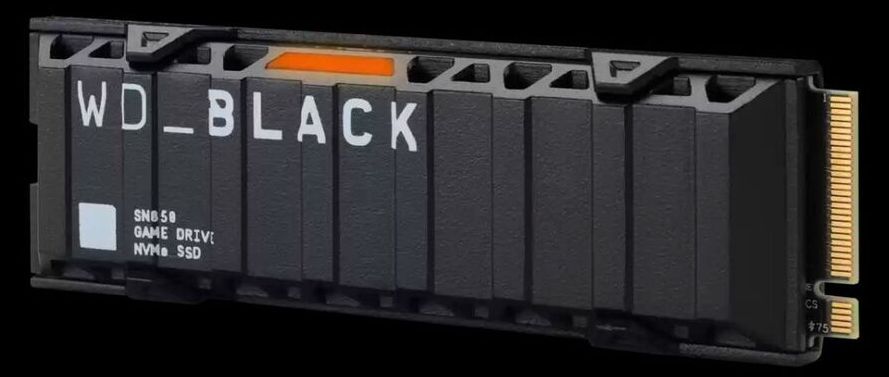
Making good on its promise, Western Digital has deployed a new firmware for the company’s WD Black SN850 SSD, which is currently one of the best SSDs on the market. The latest firmware will restore the SN850’s write performance when the drive is installed on a M.2 slot that’s connected to AMD’s X570 chipset.
The SN850 is one of the fastest SSDs around right now. However, users were reporting a performance loss of over 40% if the SSD resided on a M.2 slot that doesn’t directly communicate with the Ryzen processor. We don’t see the issue affecting users that have the SN850 as their primary drive. But for users that have multiple SSDs and have the SN850 on an M.2 slot linked to the AMD X570 chipset, it could be a huge problem.


WTF?! On Thursday the Security Service of Ukraine (SSU) reported that they had shut down a cryptomining operation in the city of Vinnytsia, seizing over 500 GPUs and 50 processors — and a bunch of Playstation 4s. Consoles built on 2013-era technology might not be great at mining, but they don’t need to be when you have 3800 of them.
Although the market for GPUs is starting to improve, and dedicated ASICs might be on the way to relieve demand, it seems that one group of enterprising cryptocurrency miners have turned to last-gen console hardware to get things done.
From the photos provided by the SSU, it looks like these consoles are of the PS4 Slim variety, the 2016 refresh of the original console from three years prior. Mostly obsolete for newer games, it’s not at all surprising that so many could be sourced en masse so easily.