This entrepreneurs immigrant parents instilled self-sufficiency. Now, he’s taking on tech giants like Apple and Microsoft by engineering a laptop anyone can build and repair on their own.
Category: computing – Page 696
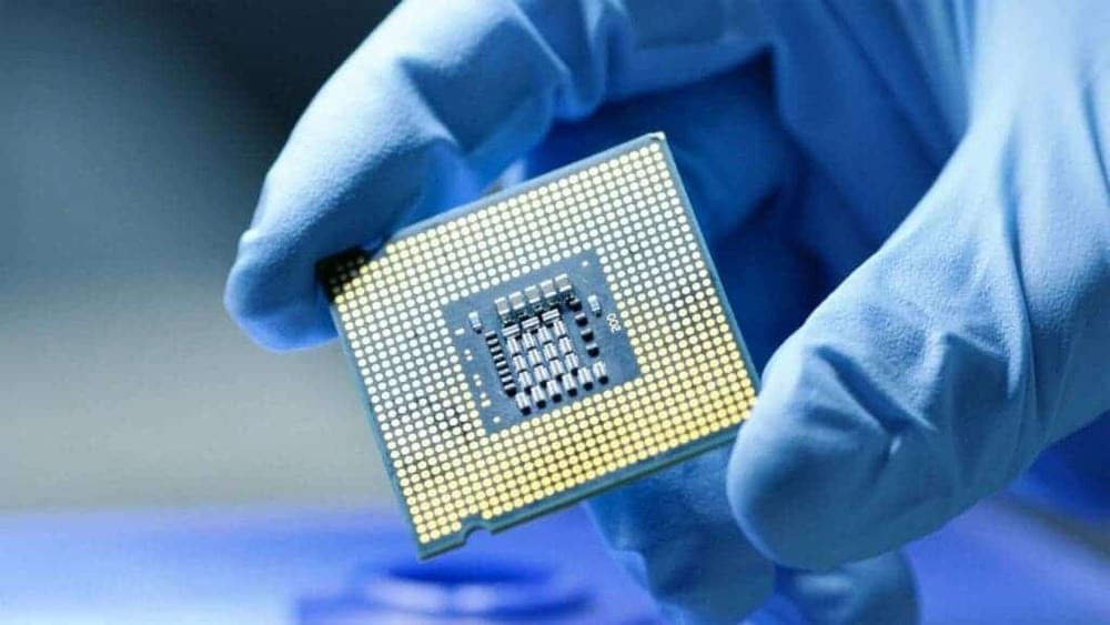
Qualcomm is set to lose top brands like Apple, Google & Samsung
According to reports, Samsung will increase the proportion of Exynos chips used in its own models in 2022 to reduce its dependence on Qualcomm chips. Samsung’s use of Exynos chips in its own models will increase by about 2–3 times next year. At the same time, Samsung has set a sales target of 300 million mobile phones next year.
Industry insiders pointed out that Samsung is vigorously supporting Exynos chips. On the one hand, it will increase the proportion of Exynos chips in its own models. On the other hand, it is open to partners. Recall that the company co-developed the Exynos 1,080 chip with Vivo which the latter used in the Vivo X60 series.
Researchers propose a simpler design for quantum computers
Today’s quantum computers are complicated to build, difficult to scale up, and require temperatures colder than interstellar space to operate. These challenges have led researchers to explore the possibility of building quantum computers that work using photons—particles of light. Photons can easily carry information from one place to another, and photonic quantum computers can operate at room temperature, so this approach is promising. However, although people have successfully created individual quantum “logic gates” for photons, it’s challenging to construct large numbers of gates and connect them in a reliable fashion to perform complex calculations.
Now, Stanford University researchers have proposed a simpler design for photonic quantum computers using readily available components, according to a paper published Nov. 29 in Optica. Their proposed design uses a laser to manipulate a single atom that in turn, can modify the state of the photons via a phenomenon called “quantum teleportation.” The atom can be reset and reused for many quantum gates, eliminating the need to build multiple distinct physical gates, vastly reducing the complexity of building a quantum computer.
“Normally, if you wanted to build this type of quantum computer, you’d have to take potentially thousands of quantum emitters, make them all perfectly indistinguishable, and then integrate them into a giant photonic circuit,” said Ben Bartlett, a Ph.D. candidate in applied physics and lead author of the paper. “Whereas with this design, we only need a handful of relatively simple components, and the size of the machine doesn’t increase with the size of the quantum program you want to run.”

Shifting Colors for On-Chip Photonics To Power Next Generation Quantum Computers and Networks
On-chip frequency shifters in the gigahertz range could be used in next generation quantum computers and networks.
The ability to precisely control and change properties of a photon, including polarization, position in space, and arrival time, gave rise to a wide range of communication technologies we use today, including the Internet. The next generation of photonic technologies, such as photonic quantum networks and computers, will require even more control over the properties of a photon.
One of the hardest properties to change is a photon’s color, otherwise known as its frequency, because changing the frequency of a photon means changing its energy.


New Platform for Quantum Computing? Artificial Material Mimics Quantum Entangled Rare Earth Compounds
Physicists have created a new ultra-thin two-layer material with quantum properties that normally require rare earth compounds. This material, which is relatively easy to make and does not contain rare earth metals, could provide a new platform for quantum computing and advance research into unconventional superconductivity and quantum criticality.
The researchers showed that by starting from seemingly common materials, a radically new quantum state of matter can appear. The discovery emerged from their efforts to create a quantum spin liquid which they could use to investigate emergent quantum phenomena such as gauge theory. This involves fabricating a single layer of atomically thin tantalum disulfide, but the process also creates islands that consist of two layers.

MX Linux has Released a New Edition for Newer Hardware
MX Linux 21 AHS is finally available with Linux Kernel 5.14 and updated open-source graphics stack. But, is it for everyone?
MX Linux 21 was officially unveiled last month while introducing a new Fluxbox edition. However, the Advanced Hardware Support (AHS) ISO was not a part of it.
Recently, MX Linux announced the availability of MX Linux 21 AHS and a new AHS repo for existing MX Linux 21 users.
In this article, let us explore more about it.
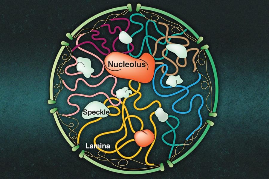
How molecular clusters in the nucleus interact with chromosomes
A cell stores all of its genetic material in its nucleus, in the form of chromosomes, but that’s not all that’s tucked away in there. The nucleus is also home to small bodies called nucleoli — clusters of proteins and RNA that help build ribosomes.
Using computer simulations, MIT chemists have now discovered how these bodies interact with chromosomes in the nucleus, and how those interactions help the nucleoli exist as stable droplets within the nucleus.
Their findings also suggest that chromatin-nuclear body interactions lead the genome to take on a gel-like structure, which helps to promote stable interactions between the genome and transcription machineries. These interactions help control gene expression.