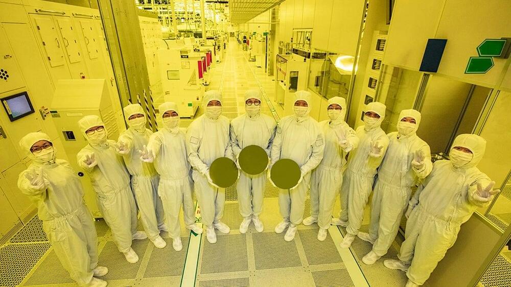
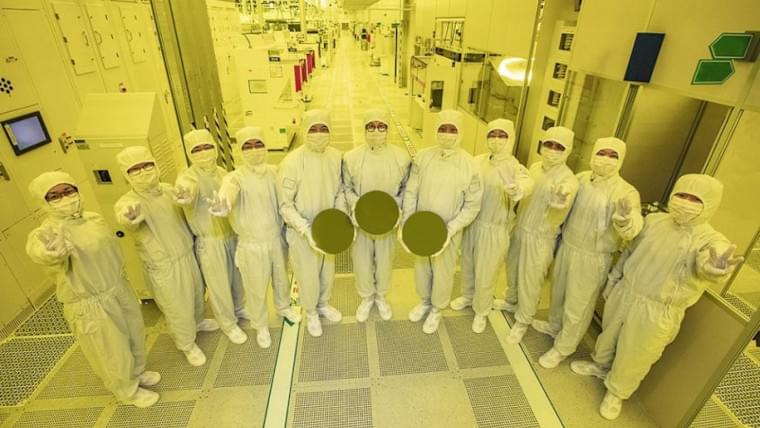
Samsung has begun mass production of chips using its 3nm process node __ its most advanced chip production technology yet that allows smaller chips to pack even more power.
“We are starting to help patients in ways that we did not think were possible,” Thomas Oxley (Mount Sinai Hospital, New York, USA) tells NeuroNews, referring to the potential of brain-computer interface (BCI) technology. Alongside his role as a vascular and interventional neurologist, Oxley is chief executive officer of Synchron, developer of the Stentrode motor neuroprosthesis. The Stentrode is an implantable BCI device that, according to Oxley, is the first of its kind to be in the early feasibility clinical stage in the USA following US Food and Drug Administration (FDA) approval of Synchron’s investigational device exemption (IDE) application last month. Speaking to NeuroNewsfollowing a presentation on the topic at the Society of NeuroInterventional Surgery’s 18thannual meeting (SNIS; 26–29 July 2021, Colorado Springs, USA and virtual), Oxley gives an overview of the COMMAND early feasibility study, anticipates key results, and considers more generally how BCI technology could shape the future of deep brain stimulation.
What if we built a Matrioshka Brain? In this video, Unveiled asks what would happen if we built a computer AROUND A STAR? This is one of the most incredible megastructures we’ve ever even contemplated… but what would the universe be like if it was home to these things? And how would we possibly keep control?
This is Unveiled, giving you incredible answers to extraordinary questions!
Find more amazing videos for your curiosity here:
What If Humanity Was A Type VII Civilization? — https://youtu.be/pz-Z8AavJZY
What If the Universe is an Atom? — https://youtu.be/WYyu9h9JJfg.
Are you constantly curious? Then subscribe for more from Unveiled ► https://wmojo.com/unveiled-subscribe.
#MatrioshkaBrain #Kardashev #Future
At present, our brains are mostly dependent on all the stuff below the neck to turn thought into action. But advances in neuroscience are making it easier than ever to hook machines up to minds. See neuroscientists John Donoghue and Sheila Nirenberg, computer scientist Michel Maharbiz, and psychologist Gary Marcus discuss the cutting edge of brain-machine interactions in “Cells to Silicon: Your Brain in 2050,” part of the Big Ideas series at the 2014 World Science Festival.
This program is part of the Big Ideas Series, made possible with support from the John Templeton Foundation.
Visit our Website: http://www.worldsciencefestival.com/
Like us on Facebook: https://www.facebook.com/worldsciencefestival.
Follow us on twitter: https://twitter.com/WorldSciFest.
Original Program date: May 29, 2014
Host: Robert Krulwich.
Participants: Gary Marcus, John Donoghue, Sheila Nirenberg, Michel M. Maharbiz.
Robert Krulwich’s Introduction. 00:11
Participant Introductions. 2:00

Blockchain is a digital technology that allows a secure and decentralized record of transactions that is increasingly used for everything from cryptocurrencies to artwork. But Yale researchers have found a new use for blockchain: they’ve leveraged the technology to give individuals control of their own genomes.
Their findings are published June 29 in the journal Genome Biology.
“Our primary goal is to give ownership of genomic data back to the individual,” said senior author Mark Gerstein, the Albert L. Williams Professor of Biomedical Informatics and professor of molecular biophysics and biochemistry, of computer science, and of statistics and data science.
LeviPrint is a system that uses acoustic manipulation for assembling objects without physical contact. It generates acoustic fields that trap small particles, glue droplets and elongated stick-like elements that can be manipulated and reoriented as they are levitated. It is a fully functional system for manufacturing 3D structures using contactless manipulation.
It was developed by researchers from the UPNA/NUP-Public University of Navarre Asier Marzo and Iñigo Ezcurdia, who together with Rafael Morales (Ultraleap Ltd, UK) and Marco Andrade (University of São Paulo, Brazil) are authors of the paper “LeviPrint: Contactless Fabrication using Full Acoustic Trapping of Elongated Parts.”
This research is due to be presented in August in Vancouver (Canada) at SIGGRAPH, a conference on computer graphics and interactive techniques where companies such as Nvidia, Disney Research and Facebook Reality Labs present their work.

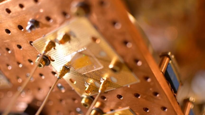
Intel Labs has announced that it has made a noteworthy advancement in the area of integrated photonics research, which it bills as the “next frontier” in expanding communications bandwidth between compute silicon in data centers and across networks. The company believes this advancement holds the promise of a future input/output (I/O) interface with improved energy efficiency and bandwidth, and a longer reach.
The disclosure explains the possibility to obtain well-matched output power in conjunction with uniform and densely spaced wavelengths, according to Haisheng Rong, Senior Principal Engineer at Intel Labs. Rong also points out that this can be done by utilizing existing manufacturing and process techniques in Intel fabs, and therefore ensures a path to volume production of the “next-generation co-packaged optics and optical compute interconnect at scale.”
Intel states that this breakthrough results in industry-leading advancements in multiwavelength integrated optics. It includes the demonstration of an eight-wavelength distributed feedback (DFB) laser array that is fully integrated on a silicon wafer and provides exceptional output power uniformity of +/-0.25 decibel (db), as well as wavelength spacing uniformity of +/-6.5% that go beyond industry specifications.