Archive for the ‘computing’ category: Page 625
May 18, 2019
How data centers will breathe life into 5G
Posted by Shailesh Prasad in categories: computing, internet, mobile phones, virtual reality
Is the future finally here? The arrival of 5G (fifth generation mobile networks) has been keenly anticipated and long discussed. And if you attended the latest Mobile World Congress, held in Barcelona in February, you would have seen plenty to suggest that 5G will take off in 2019. Smartphone manufacturers are busy preparing their 5G models, the wireless networks on which they will run are being planned, and there is no shortage of visionary use cases highlighting how virtual reality and other technologies will harness 5G’s amazing power and connectivity. In short, our lives are about to change.
May 18, 2019
Samsung at foundry event talks about 3nm, MBCFET developments
Posted by Klaus Baldauf in category: computing
“The nanometer process deals with the space between the transistors mounted on a substrate at a nanometer level,” said Pulse.
“The narrower the distance, the more chips can be squeezed in to boost computing power and energy efficiency. One nanometer corresponds to one ten-thousandth the diameter of a human hair.”
Continue reading “Samsung at foundry event talks about 3nm, MBCFET developments” »
May 17, 2019
Ultra-clean fabrication platform produces nearly ideal 2-D transistors
Posted by Quinn Sena in categories: business, computing, engineering, particle physics
Semiconductors, which are the basic building blocks of transistors, microprocessors, lasers, and LEDs, have driven advances in computing, memory, communications, and lighting technologies since the mid-20th century. Recently discovered two-dimensional materials, which feature many superlative properties, have the potential to advance these technologies, but creating 2-D devices with both good electrical contacts and stable performance has proved challenging.
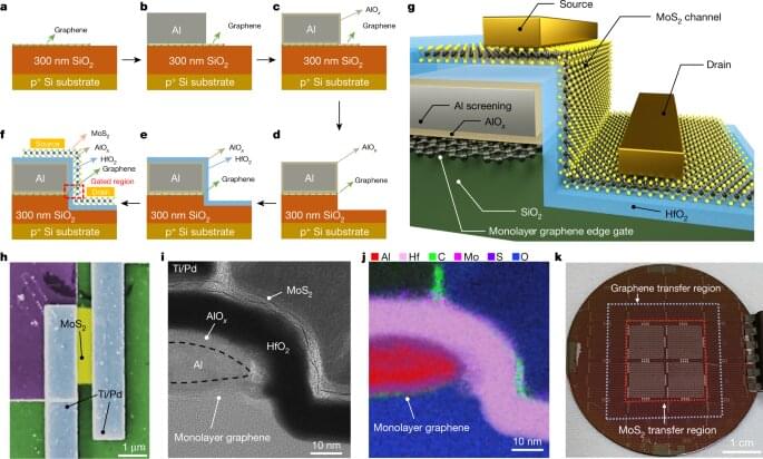
Researchers at Columbia Engineering report that they have demonstrated a nearly ideal transistor made from a two-dimensional (2-D) material stack—with only a two-atom-thick semiconducting layer—by developing a completely clean and damage-free fabrication process. Their method shows vastly improved performance compared to 2-D semiconductors fabricated with a conventional process, and could provide a scalable platform for creating ultra-clean devices in the future. The study was published today in Nature Electronics.
Continue reading “Ultra-clean fabrication platform produces nearly ideal 2-D transistors” »
May 17, 2019
NIST team demonstrates heart of next-generation chip-scale atomic clock
Posted by Quinn Sena in categories: computing, particle physics, satellites
Physicists at the National Institute of Standards and Technology (NIST) and partners have demonstrated an experimental, next-generation atomic clock—ticking at high “optical” frequencies—that is much smaller than usual, made of just three small chips plus supporting electronics and optics.
Described in Optica, the chip-scale clock is based on the vibrations, or “ticks,” of rubidium atoms confined in a tiny glass container, called a vapor cell, on a chip. Two frequency combs on chips act like gears to link the atoms’ high-frequency optical ticks to a lower, widely used microwave frequency that can be used in applications.
The chip-based heart of the new clock requires very little power (just 275 milliwatts) and, with additional technology advances, could potentially be made small enough to be handheld. Chip-scale optical clocks like this could eventually replace traditional oscillators in applications such as navigation systems and telecommunications networks and serve as backup clocks on satellites.
Continue reading “NIST team demonstrates heart of next-generation chip-scale atomic clock” »
May 17, 2019
Amazing Device Turns Thoughts Into Audible Sentences
Posted by Quinn Sena in categories: computing, neuroscience
May 17, 2019
A New Ion-Drive Transistor Is Here to Interface With Your Brain
Posted by Quinn Sena in categories: biotech/medical, computing, cyborgs, neuroscience
Silicon transistors and the brain don’t mix.
At least not optimally. As scientists and companies are increasingly exploring ways to interface your brain with computers, fashioning new hardware that conforms to and compliments our biological wetware becomes increasingly important.
To be fair, silicon transistors, when made into electrode arrays, can perform the basics: record neural signals, process and analyze them with increasingly sophisticated programs that detect patterns, which in turn can be used to stimulate the brain or control smart prosthetics.
Continue reading “A New Ion-Drive Transistor Is Here to Interface With Your Brain” »
May 17, 2019
Manipulating atoms one at a time with an electron beam
Posted by Quinn Sena in categories: computing, engineering, particle physics, quantum physics
The ultimate degree of control for engineering would be the ability to create and manipulate materials at the most basic level, fabricating devices atom by atom with precise control.
Now, scientists at MIT, the University of Vienna, and several other institutions have taken a step in that direction, developing a method that can reposition atoms with a highly focused electron beam and control their exact location and bonding orientation. The finding could ultimately lead to new ways of making quantum computing devices or sensors, and usher in a new age of “atomic engineering,” they say.
The advance is described today in the journal Science Advances, in a paper by MIT professor of nuclear science and engineering Ju Li, graduate student Cong Su, Professor Toma Susi of the University of Vienna, and 13 others at MIT, the University of Vienna, Oak Ridge National Laboratory, and in China, Ecuador, and Denmark.
Continue reading “Manipulating atoms one at a time with an electron beam” »
May 17, 2019
XPS 15 2-in-1’s maglev keyboard may find its way into other Dell laptops — Frank Azor
Posted by Quinn Sena in categories: computing, entertainment
Much ado has been made of Dell’s new maglev keyboard, currently exclusive to the XPS 15 9575 2-in-1. Utilizing rare-earth magnets to repulse the keys back up once depressed, the keyboard still provides a decent amount of feedback despite its meager 0.7mm of travel.
In a late March webcast for Dell’s new products, the company’s Vice President & General Manager Alienware, Gaming and XPS, Frank Azor, mentioned that the keyboard could be adopted in more of Dell’s laptops — if it proves popular.
The major advantage of design is that it allows the laptop to be thinner, but not everyone is a fan. Though it provides more travel and feedback than Apple’s much-maligned “butterfly” keyboard, initial reviews suggest that the keyboard is basically tolerable, but it isn’t going to replace a ThinkPad’s keyboard anytime soon.
May 17, 2019
Laptops to get maglev keyboards that reduce their thickness
Posted by Quinn Sena in category: computing
Magnetic levitation keyboards have been around for a while, but they’ve never really taken off, or floated our boats, or attracted much atten… Anyway, a Taiwanese manufacturer called Darfon is persevering with the idea, and it’s discovered that maglev keys, which rest on opposing magnets instead of mushy membranes or mechanical switches, can make laptop keyboards significantly thinner. Unfortunately, according to a CNET journalist who played with a couple of prototypes at Computex, the keys can be hard to type on if skinniness is taken to the extreme. Then again, there’s scope to change the resistance of the keyboard electronically to suit your preference, and Darfon claims it has already received orders from laptop makers who are targeting launches later this year. If that’s true, perhaps the technology isn’t so repellant after all.
[Image credit: Aloysius Low / CNET].