Microplastics, tiny particles of plastic that are now found worldwide in the air, water, and soil, are increasingly recognized as a serious pollution threat, and have been found in the bloodstream of animals and people around the world.
An Israeli security researcher has demonstrated a novel attack against air-gapped systems by leveraging the SATA cables inside computers as a wireless antenna to emanate data via radio signals.
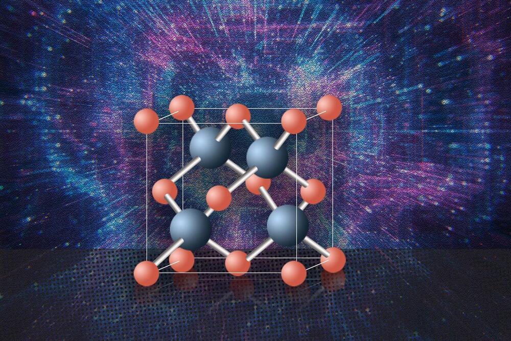
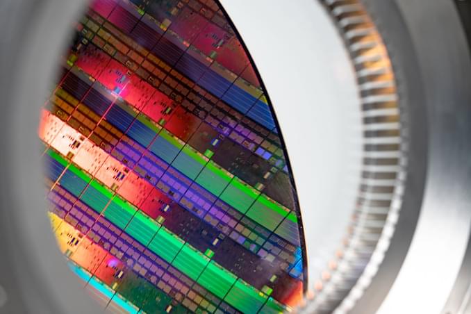
Silicon is one of the most abundant elements on Earth, and in its pure form the material has become the foundation of much of modern technology, from solar cells to computer chips. But silicon’s properties as a semiconductor are far from ideal.
For one thing, although silicon lets electrons whizz through its structure easily, it is much less accommodating to “holes”—electrons’ positively charged counterparts—and harnessing both is important for some kinds of chips. What’s more, silicon is not very good at conducting heat, which is why overheating issues and expensive cooling systems are common in computers.
Now, a team of researchers at MIT, the University of Houston, and other institutions has carried out experiments showing that a material known as cubic boron arsenide overcomes both of these limitations. It provides high mobility to both electrons and holes, and has excellent thermal conductivity. It is, the researchers say, the best semiconductor material ever found, and maybe the best possible one.


This mind-bending property offers a sought-after benefit: Information stored in the phase is far more protected against errors than with alternative setups currently used in quantum computers. As a result, the information can exist without getting garbled for much longer, an important milestone for making quantum computing viable, says study lead author Philipp Dumitrescu.
The approach’s use of an “extra” time dimension “is a completely different way of thinking about phases of matter,” says Dumitrescu, who worked on the project as a research fellow at the Flatiron Institute’s Center for Computational Quantum Physics in New York City. “I’ve been working on these theory ideas for over five years, and seeing them come actually to be realized in experiments is exciting.”
Metamaterial Space Applications:
In this presentation I will talk about nanophotonics, more specifically metasurfaces – subwavelength patterned surfaces – and explain how this can be used for space applications. As recently displayed by the stunning images from the James Webb space telescope, we often rely on recording the intensity of light (e.g. with a camera) to study the universe. However, light fundamentally has several additional degrees of freedom which can carry information, e.g. polarization, phase, and spectral content. While it is true that many conventional optical components can address these degrees of freedom individually (e.g., polarizers, phase retarders, and filters), metasurfaces enable general manipulations of phase, amplitude, and polarization on the nanoscale, thereby providing ample opportunity to create new versions of existing components and even enable functionality not possible using conventional technologies. In the presentation I will cover several examples of metasurfaces I have been working on and explain their relevance for space applications. I will attempt to explain the working principles, why metasurfaces can be useful, as well as how we fabricate metasurfaces in a cleanroom.
About the speaker: Dr. Tobias Wenger is a postdoc at JPL’s microdevices laboratory (MDL) where his main efforts relate to nanophotonics — light at the nanoscale – and how we can engineer structures and components in order to control light in new ways. Tobias received his PhD from Chalmers University of Technology, Sweden, where he worked on understanding the physical properties of plasmons in graphene.
At JPL, Tobias is applying his knowledge of subwavelength electromagnetics to design metasurface-based optical components, mainly for infrared wavelengths. Metasurfaces are a novel approach to optics which uses subwavelength elements for controlling the phase, amplitude and polarization of transmitted and/or reflected electromagnetic radiation. Tobias research interests intersect optics, computational electromagnetics, and microfabrication and he enjoys both the practical and theoretical aspects of this work. During his postdoc time at MDL, he has worked on metasurface-based optical concentrators, IR detectors, plasmonic filters, wavefront sensing, and grating replication.

Circa 2021 force field this can also shield the earth or cities.
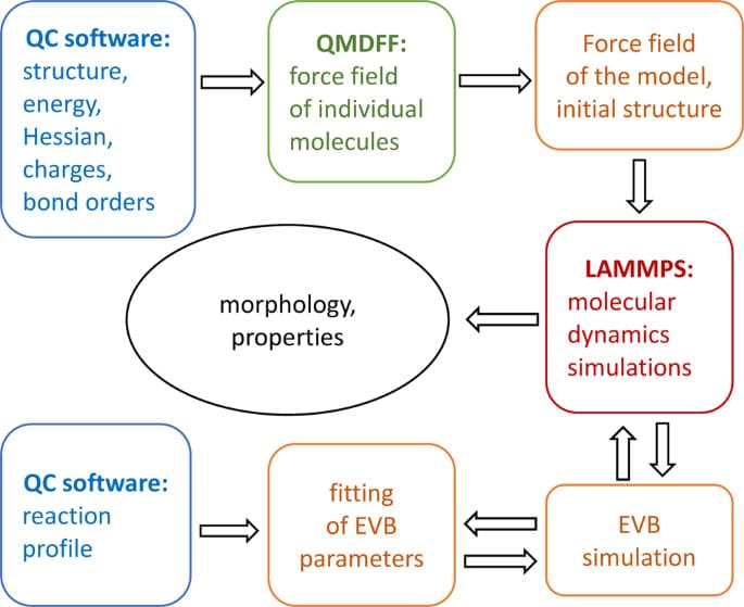
The computational design of functional materials relies heavily on large-scale atomistic simulations. Such simulations are often problematic for conventional classical force fields, which require tedious and time-consuming parameterization of interaction parameters. The problem can be solved using a quantum mechanically derived force field (QMDFF)—a system-specific force field derived directly from the first-principles calculations. We present a computational approach for atomistic simulations of complex molecular systems, which include the treatment of chemical reactions with the empirical valence bond approach. The accuracy of the QMDFF is verified by comparison with the experimental properties of liquid solvents.