Toggle light / dark theme

Experimental photonic quantum memristor

We have designed an optical memristive element that allows the transmission of coherent quantum information as a superposition of single photons on spatial modes. We have realized the prototype of such a device on a glass-based, laser-written photonic processor and thereby provided what is, to the best of our knowledge, the first experimental demonstration of a quantum memristor. We have then designed a memristor-based quantum reservoir computer and tested it numerically on both classical and quantum tasks, achieving strong performance with very limited physical and computational resources and, most importantly, no architectural change from one to the other.

Our demonstrated quantum memristor is feasible in practice and readily scalable to larger architectures using integrated quantum photonics, with immediate feasibility in the noisy intermediate-scale quantum regime. The only hard limit for larger scalability—as with most quantum photonic applications—is the achievable single-photon rate. A foreseeable advancement would be the integration of optical and electronic components within the same chip (rather than using external electronics), which is conceivable using current semiconductor technology. Additionally, the frequency at which our quantum memristor operates can be easily improved. For laser-written circuits, high-frequency operations are readily available at the expense of higher-power consumption28, whereas other photonic platforms routinely enable frequencies even in the gigahertz regime43. For exploiting these frequencies, however, the photon detection rate must be improved as well.

Stretchy light-emitting plastic could be used in wearable screens

An elastic light-emitting polymer that glows like a filament in a light bulb could lead to affordable, practical and robust flexible screens.

Flexible screens could form part of wearable computers that stick to our skin and do away with the need to carry a separate smartphone or laptop. But the various existing flexible displays all have flaws: they either require high voltages to run, are too fragile, too expensive, not bendy enough or lack brightness.

New technique opens door to cheaper semiconductors, higher chip yield

Scientists from the NTU Singapore and the Korea Institute of Machinery & Materials (KIMM) have developed a technique to create a highly uniform and scalable semiconductor wafer, paving the way to higher chip yield and more cost-efficient semiconductors.

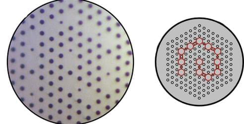
Left: Image of a six-inch silicon wafer with printed metal layers and its top-view scanning electron microscope image. Right: Image of the six-inch silicon wafer with nanowires and its cross-sectional scanning electron microscope image. (Image: NTU Singpore)

Semiconductor chips commonly found in smart phones and computers are difficult and complex to make, requiring highly advanced machines and special environments to manufacture.

A new class of materials for nanopatterning

The microscopic components that make up computer chips must be made at staggering scales. With billions of transistors in a single processor, each made of multiple materials carefully arranged in patterns as thin as a strand of DNA, their manufacturing tools must also operate at a molecular level.

Typically, these tools involve using stencils to selectively pattern or remove materials with high fidelity, layer after layer, to form nanoscale electronic devices. But as chips must fit more and more components to keep up with the digital world’s growing computational demands, these nanopatterning stencils must also become smaller and more precise.

Now, a team of Penn Engineers has demonstrated how a new class of polymers could do just that. In a new study, the researchers demonstrated how “multiblock” copolymers can produce exceptionally ordered patterns in thin films, achieving spacings smaller than three nanometers.

How Can Quantum Computing Change the World?

Every industry will be affected by quantum computing. They will alter the way business is done and the security systems in place which protect data, how we battle illnesses and create new materials, as well as how we tackle health and climate challenges.

As the race to build the first commercially functional quantum computer heats up, here we discuss a handful of the ways quantum computing will alter our world.

The future of PSUs is here: Intel’s ATX 3.0 powers monster 600W graphics cards

PC power supplies haven’t seen a whole lot of change in the last decade or two. We’ve gotten modular cables for easier routing, smaller standards for itty-bitty builds, and that’s about it. But today Intel has finalized the ATX 3.0 standard, coming soon to a full-sized PC case near you. The biggest addition announced today is a new standardized connection for graphics cards and other PCIe devices, delivering up to 600 watts on a single connector.

Currently graphics cards are in a bit of a power pinch. The maximum throughput for an 8-pin ATX rail is 150 watts, so the biggest and most power-hungry GPUs need to double or even triple up, adding extra space requirements and more complex cable routing inside the case. The new 12-pin 12VHPWR connection should be able to deliver more energy than even the most powerful graphics cards need for the next generation or two. Each pin housing is also physically smaller, with a 3.0mm pitch versus 4.2mm on current power supply rails.

Technically it’s 16 total pins (12+4), with four additional data pins squeezed in beneath the primary power pins. This is to manage DC output voltage regulation and a series of new tools designed to regulate high power output efficiently and safely, all handled intelligently by the power supply. According to Intel, the new 12VHPWR connection will be the standard for “most, if not all” PCIe cards using the 5.0 spec.

Direct generation of complex structured light

Extension of laser beam structures promises new laser applications. Exploration of how beam structures change during nonlinear frequency conversion processes has drawn increasing interest in recent years. Nonlinear conversion is an excellent route for structured beam generation and represents a growing, hybrid field for researchers in nonlinear optics and laser technology, as well as the emerging area of light-field regulation technology.

For structured and nonlinear frequency conversion, researchers have considered both intracavity oscillation and external cavity spatial modulation. To achieve flexible outputs, spatial light modulators can be used to obtain structured beams both inside and outside the cavity. But this is an indirect, inefficient method. Intracavity nonlinear frequency generation of structured beams offers a direct, efficient method that has only rarely been investigated, until recently.

Inside a laser cavity, an effect known as “transverse mode locking” (TML) enables the direct generation of the vortex beams or optical vortices from a laser cavity. It is known that both solid-state microchip lasers and VCSELs can produce quite similar outputs of TML beam patterns under large Fresnel number pumping conditions. The complex transverse patterns formed by the TML effect, commonly composed of different basic modes with different weight coefficients and different locking phases, make for abundant spatial information in fundamental frequency modes. Nonlinear frequency conversion of these directly generated TML beams is of great interest, but not yet well studied.

/* */