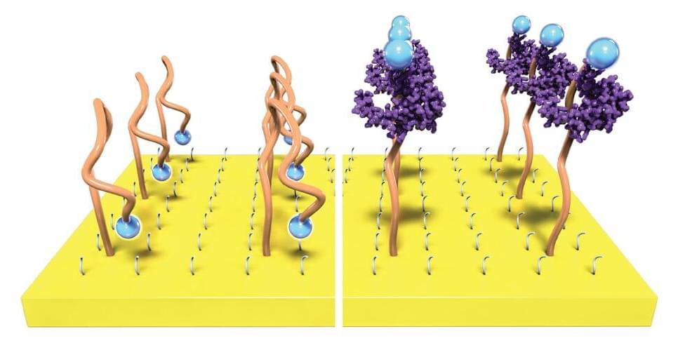
Organic transistors that can simulate basic synaptic functions and act as biomimetic devices are advantageous for next generation bioelectronics. Here, the authors realize non-volatile organic electrochemical transistors with optimized performance required for associative learning circuits.
Category: computing – Page 495
A new way to form self-aligned ‘color centers’ promises scalability to over 10000 qubits for applications in quantum sensing and quantum computing.
Achieving the immense promise of quantum computing requires new developments at every level, including the computing hardware itself. A Lawrence Berkeley National Laboratory (Berkeley Lab)-led international team of researchers has discovered a way to use ion beams to create long strings of “color center” qubits in diamond. Their work is detailed in the journal Applied Physics Letters.
The authors includes several from Berkeley Lab: Arun Persaud, who led the study, and Thomas Schenkel, head of the Accelerator Technology and Applied Physics (ATAP) Division’s Fusion Science & Ion Beam Technology Program, as well as Casey Christian (now with Berkeley Lab’s Physics Division), Edward Barnard of Berkeley Lab’s Molecular Foundry, and ATAP affiliate Russell E. Lake.
IBM has built the first 2nm wafers in the semiconductor industry, several years before the node is expected to hit commercial volumes.
Harnessing the Hum of Fluorescent Lights for More Efficient Computing
The property that makes fluorescent lights buzz could power a new generation of more efficient computing devices that store data with magnetic fields, rather than electricity.
A team led by University of Michigan researchers has developed a material that’s at least twice as “magnetostrictive” and far less costly than other materials in its class. In addition to computing, it could also lead to better magnetic sensors for medical and security devices.
Moore’s Law, the famous prediction that the number of transistors that can be packed onto a microchip will double every couple of years, has been bumping into basic physical limits. These limits could bring decades of progress to a halt, unless new approaches are found.
One new direction being explored is the use of atomically thin materials instead of silicon as the basis for new transistors, but connecting those “2D” materials to other conventional electronic components has proved difficult.
Now researchers at MIT, the University of California at Berkeley, the Taiwan Semiconductor Manufacturing Company, and elsewhere have found a new way of making those electrical connections, which could help to unleash the potential of 2D materials and further the miniaturization of components—possibly enough to extend Moore’s Law, at least for the near future, the researchers say.
Scientists used to perform experiments by stirring biological and chemical agents into test tubes.
Nowadays, they automate research by using microfluidic chips the size of postage stamps. In these tiny devices, millions of microscopic particles are captured in droplets of water, each droplet serving as the “test tube” for a single experiment. The chip funnels these many droplets, one at a time, through a tiny channel where a laser probes each passing droplet to record thousands of experimental results each second.
These chips are used for such things as testing new antibiotics, screening drug compounds, sequencing the DNA and RNA of single cells, and otherwise speeding up the pace of scientific discovery.
By decoding the brain signals involved in handwriting, researchers have allowed a man who is paralyzed to transform his thoughts into words on a computer screen.
Eight months on, the semiconductor shortage seems likely to stretch into 2022. Increasing chip production is a slow and difficult business.
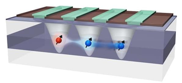
Intel has overcome a quantum computing bottleneck by controlling two qubits with a cryogenic control chip.