Advantageously, the fabrication of OECTs, in particular of the conductive channel, is compatible with solution-based fabrication methods and additive manufacturing, enabling cost-efficient manufacturing and rapid prototyping on flexible substrates10. This opens new possibilities in terms of the combination of materials that can be used in the manufacturing of OECTs, in particular the use of degradable materials. Degradable electronics refer to electronic systems and components that can degrade in an environment of interest spontaneously, in a controlled amount of time, and without releasing byproducts that are harmful to that environment18. With concerning amounts of electronic waste being generated, as well as exploding numbers of connected Internet of Things (IoT) devices19, there is growing interest in transient electronic systems with a service life of a few days to a few months. Although advances have been made in the manufacturing of fully degradable functional devices, i.e. antennas20, batteries21 and physical as well as environmental sensors22,23, investigations into degradable biosensors remain relatively limited24.
Advances have been made in proposing new materials for the OECT terminals, in particular the gate electrode, as its properties play a key role in modulating the transistor’s behavior. While Ag/AgCl gates offer the advantage of being non-polarizable, Au gates present little electrochemical activity in the range of voltages typical for OECT-based biosensing. Au and PEDOT: PSS gates have been explored for OECT-based biosensors, with the advantage of expanding the possibilities for bio-functionalizing the gate electrode6,25. PEDOT: PSS gates and contacts have been investigated, simplifying notably their manufacturing26. An all-PEDOT: PSS OECT was presented and shown to measure dopamine concentrations reliably and specifically27. Various forms of carbon have also been investigated for the realization of gate electrodes for OECTs8. Activated carbon gates, for example, showed increased drain current modulation due to the large specific surface area of the carbon material9. Recently, screen-printed carbon-gated OECTs were shown to be suitable for the detection of uric acid after functionalization of the carbon gate with platinum and Uricase28. Transient or recyclable materials such as paper26 have been proposed as substrates for OECTs. Polylactic acid (PLA)24 and Poly(lactic-co-glycolic acid)29 (PLGA) have been studied as degradable substrates for OECTs30, as well as diacetate cellulose31. These studies, however, relied on non-degradable contacts for the operation of the printed OECTs. More recently, Khan et al.32 proposed a fully printed OECT on cellulose acetate (CA) for the selective detection of glucose. The OECT is made of degradable materials and CA is a biocompatible material that is suitable as a substrate for transient biosensors.
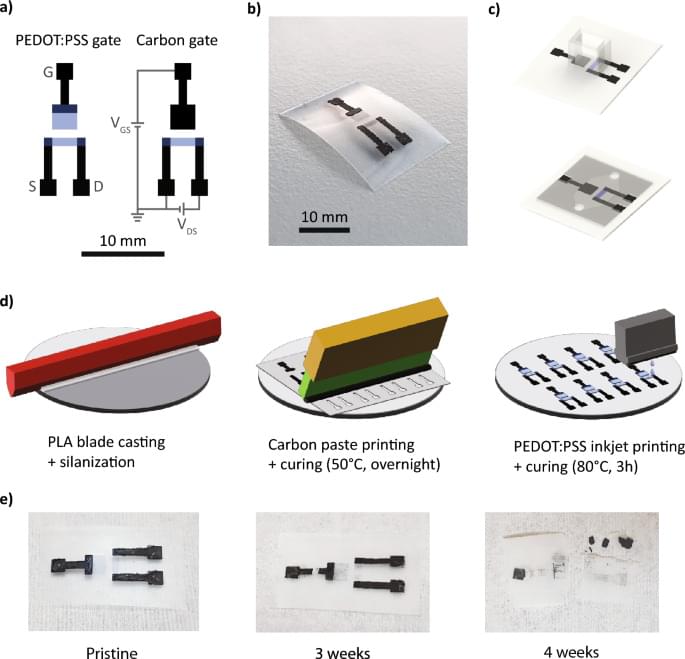
In this work, we present disposable and biocompatible OECTs based on carbon, PEDOT: PSS and PLA as substrate. Challenges in the fabrication of transient electronic devices come from the low-temperature tolerance18 of biopolymeric substrates and reaching adhesion of the PEDOT: PSS channel material on the biopolymer33, which is often deposited from an aqueous solution. A fully additive fabrication process is developed to address these challenges, leveraging screen and inkjet printing. The influence of the gate material choice, as well as the gate geometry, are studied, and these parameters are optimized for the fabrication of transient OECTs for ions and metabolite sensing. The transistor characteristics of the devices as well as their sensing behavior and reproducibility are characterized. Finally, the degradable OECTs are integrated with highly conductive transient zinc metal traces, which are of interest for interconnection with other degradable electronic circuits and could allow, for example, the wireless operation of the biochemical chemical sensors34.


