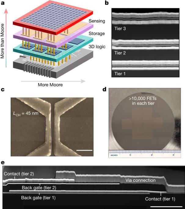
Monolithic three-dimensional integration of two-dimensional field-effect transistors enables improved integration density and multifunctionality to realize ‘More Moore’ and ‘More than Moore’ technologies.


QuEra, a quantum computing startup founded by researchers from Harvard and the Massachusetts Institute of Technology, recently released what may be the most ambitious quantum technology roadmap we’ve seen yet.
The company plans on releasing a quantum computer with 100 logical qubits and 10,000 physical qubits by 2026. It also claims this planned system will demonstrate “practical quantum advantage,” meaning they’d be capable of useful computation feats that classical, binary computers aren’t.

Producing photons one at a time on demand at room temperature is a key requirement for the rollout of a quantum internet—and the practical quantum computers that would undergird that network. The photons can be used as quantum bits (qubits), the quantum equivalent of classical computing’s 0s and 1s. Labs around the world have devised various ways to generate single photons, but they can involve complex engineering techniques such as doped carbon nanotubes or costly cryogenically-cooled conditions. On the other hand, less complicated techniques such as using traditional light sources do not provide the necessary level of control over single-photon emissions required for quantum networks and computers.
Now, researchers from Tokyo University of Science (TUS) and the Okinawa Institute of Science and Technology have collaborated to develop a prototype room temperature single-photon light source using standard materials and methods. The team described the fabrication of the prototype and its results in a recent issue of the journal Physical Review Applied.
“Our single-photon light source … increases the potential to create quantum networks—a quantum internet—that are cost-effective and accessible.” —Kaoru Sanaka, Tokyo University of Science.

The research conducted by Elena Hassinger, an expert in low-temperature physics working at ct.qmat—Complexity and Topology in Quantum Matter (a joint initiative by two universities in Würzburg and Dresden), has always been synonymous with extreme cold.
In 2021, she discovered the unconventional superconductor cerium-rhodium-arsenic CeRh2As2). Superconductors normally have just one phase of resistance-free electron transport, which occurs below a certain critical temperature. However, as reported in the academic journal Science, CeRh2As2 is so far the only quantum material to boast two certain superconducting states.
Lossless current conduction in superconductors has remained a central focus in solid-state physics for decades and has emerged as a significant prospect for the future of power engineering. The discovery of a second superconducting phase in CeRh2As2, which results from an asymmetric crystal structure around the cerium atom (the rest of the crystal structure is completely symmetrical), positions this compound as a prime candidate for use in topological quantum computing.
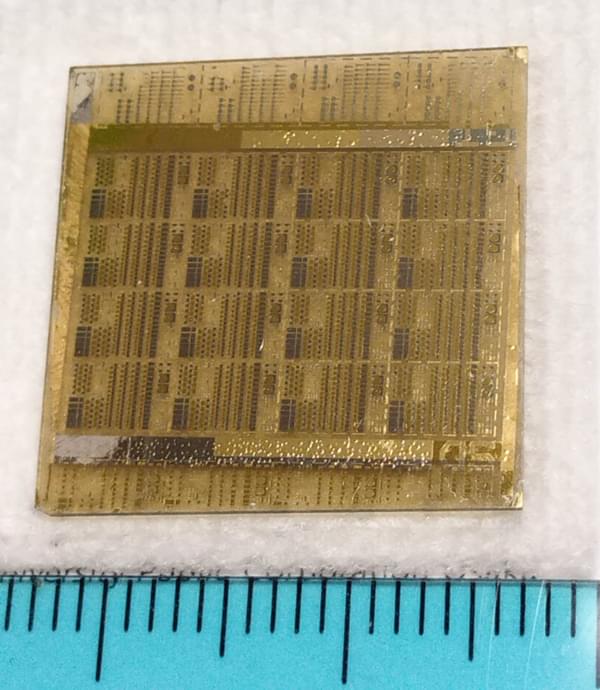
A research team at Osaka Metropolitan University has fabricated a gallium nitride (GaN) transistor using diamond, which of all natural materials has the highest thermal conductivity on earth, as a substrate, and they succeeded in increasing heat dissipation by more than 2X compared with conventional transistors. The transistor is expected to be useful not only in the fields of 5G communication base stations, weather radar, and satellite communications, but also in microwave heating and plasma processing.
Researchers at Osaka Metropolitan University are proving that diamonds are so much more than just a ‘girl’s best friend.’ Their groundbreaking research focuses on gallium nitride (GaN) transistors, which are high-power, high-frequency semiconductor devices used in mobile data and satellite communication systems.
With the increasing miniaturization of semiconductor devices, problems arise such as increases in power density and heat generation that can affect the performance, reliability, and lifetime of these devices.
Explore the digital archaeology of computing’s past with the unearthing of 86-DOS version 0.1-C, the oldest ancestor of MS-DOS
A code archaeologist has unearthed a treasure trove for tech historians: the oldest-known ancestor of Microsoft’s iconic MS-DOS.
Discover the hidden gems of computing history as a code enthusiast shares the earliest-known iteration of 86-DOS online from an archive.
Although chaos theory can solve nearly anything that is unknown I basically think that in an infinite universe as made real from the infinite microchip that uses superfluid processing power is the real answer and we are off by factor of infinite parameters still.
When we look at scientific progress, especially in physics, it can seem like all the great discoveries lie behind us. Since the revolutions of Einstein’s theory of relativity and quantum mechanics, physicists have been struggling to find a way to make them fit together with little to no success. Tim Palmer argues that the answer to this stalemate lies in chaos theory.
Revisiting a book by John Horgan, science communicator and theoretical physicist Sabine Hossenfelder recently asked on her YouTube channel whether we are facing the end of science. It might seem like a rhetorical question — it’s not possible for science to really end — but she concludes that we are in dire need of some new paradigms in physics, and seemingly unable to arrive at them. We are yet to solve the deep ongoing mysteries of the dark universe and still haven’t convincingly synthesised quantum and gravitational physics. She suggests that ideas from chaos theory might hold some of the answers, and therefore the ability to rejuvenate science. I think she’s right.
Many physicists – perhaps most — might think this is surely a silly idea. After all, chaotic systems are describable by elementary classical Newtonian dynamics. The phenomenon of chaos can be illustrated by taking the simplest of dynamical systems, the pendulum, and simply adding a second pivot into its swinging arm. The motion of the tip of the pendulum arm is hard to predict, being sensitive to its exact starting conditions – the hallmark of chaos. Fascinating yes, but surely, if we have learned anything over the last 100 years it is this: we are not going to make progress in fundamental physics by going back to elementary classical dynamics.
The first functional semiconductor made from graphene has been created at the Georgia Institute of Technology. This could enable smaller and faster electronic devices and may have applications for quantum computing.
Credit: Georgia Institute of Technology.
Semiconductors, which are materials that conduct electricity under specific conditions, are foundational components of electronic devices like the chips in your computer, laptop, and smartphone. For many decades, their architecture has been getting smaller and more compact – a trend known as Moore’s Law. This has enabled gigantic leaps in a vast range of technologies, from general computing speeds and video game graphics, to the resolution of medical scans and the sensitivity of astronomical observatories.