Toggle light / dark theme

Article originally published on LINKtoLEADERS under the Portuguese title “Sem saber ler nem escrever!”

In the 80s, “with no knowledge, only intuition”, I discovered the world of computing. I believed computers could do everything, as if it were an electronic God. But when I asked the TIMEX Sinclair 1000 to draw the planet Saturn — I am fascinated by this planet, maybe because it has rings —, I only glimpse a strange message on the black and white TV:

In this video I discuss 5 Types of Compute which can replace our traditional Computers in the Future.

Watch Next:
➞ Analog Compute: https://youtu.be/f4A85foHPZY
➞ Biological Compute: https://youtu.be/FuzoLdrRX5Q
➞ Compute with Light: https://youtu.be/mt8I71VUazw.
➞ Quantum Computers: https://youtu.be/j9eYQ_ggqJk.
➞ RF compute paper: https://www.researchgate.net/publication/345970494_Radio-Fre…c_Synapses.

➞ Support me on Patreon: https://www.patreon.com/AnastasiInTech.
➞ Subscribe to my Newsletter: https://anastasiintech.substack.com

A household microwave oven modified by a Cornell engineering professor is helping to cook up the next generation of cellphones, computers and other electronics after the invention was shown to overcome a major challenge faced by the semiconductor industry.

The research is detailed in a paper published in Applied Physics Letters. The lead author is James Hwang, a research professor in the department of materials science and engineering.

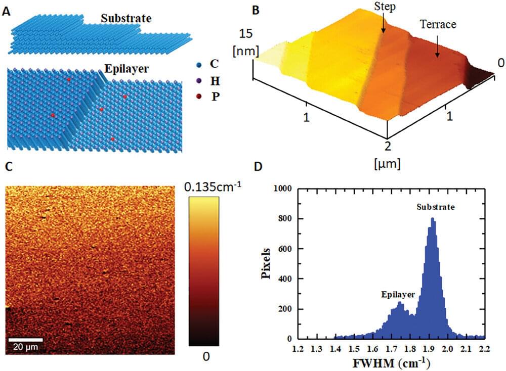
As microchips continue to shrink, silicon must be doped, or mixed, with higher concentrations of phosphorus to produce the desired current. Semiconductor manufacturers are now approaching a critical limit in which heating the highly doped materials using traditional methods no longer produces consistently functional semiconductors.

Skin-like electronics could seamlessly integrate with the body for applications in health monitoring, medication therapy, implantable medical devices, and biological studies.

With the help of the Polsky Center for Entrepreneurship and Innovation, Sihong Wang, an assistant professor of molecular engineering at the University of Chicago’s Pritzker School of Molecular Engineering, has secured patents for the building blocks of these novel devices.

Drawing on innovation in the fields of semiconductor physics, solid mechanics, and energy sciences, this work includes the creation of stretchable polymer semiconductors and transistor arrays, which provide exceptional electrical performance, high semiconducting properties, and mechanical stretchability. Additionally, Wang has developed triboelectric nanogenerators as a new technology for harvesting energy from a user’s motion—and designed the associated energy storage process.

Over the last decade, improvements in optical atomic clocks have repeatedly led to devices that have broken records for their precision (see Viewpoint: A Boost in Precision for Optical Atomic Clocks). To achieve even better performance, physicists must find a way to cool the atoms in these clocks to lower temperatures, which would allow them to use shallower atom traps and reduce measurement uncertainty. Tackling this challenge, Xiaogang Zhang and colleagues at the National Institute of Standards and Technology, Colorado, have cooled a gas of ytterbium atoms to a record low temperature of a few tens of nanokelvin [1]. As well as enabling the next generation of optical atomic clocks, the researchers say that their technique could be used to cool atoms in neutral-atom quantum computers.

Divalent atoms such as ytterbium are especially suited to precision metrology, as their lack of net electronic spin makes them less sensitive than other species to environmental noise. These atoms can be cooled to the necessary sub-µK temperatures in several ways, but not all techniques are compatible with the requirements of high-precision clocks. For example, evaporative cooling, in which the most energetic atoms are removed, is time-consuming and depletes the atoms. Meanwhile, resolved sideband cooling chills the motion of the atoms only along the axis of the 1D optical trap, leaving their off-axis motion unaffected.

Zhang and colleagues cool their atoms using a laser tuned to ytterbium’s so-called clock transition, whose extremely narrow linewidth means that the atom can theoretically be cooled to below 10 nK. They demonstrate that the precision of a clock employing a shallow lattice trap enabled by such a temperature would not be limited by atoms tunneling between adjacent lattice sites, potentially allowing a measurement uncertainty below 10-19.

South Korea’s Samsung Electronics has launched a new and its largest chip production line. The new factory was opened in Pyeongtaek, South Korea, 70 km from Seoul.

Here’s what we know

Despite the September 7 launch, the P3 line began operating as early as mid-summer. Samsung started trial production of NAND memory in July. The new facility uses ASML’s lithography machines. It is the dutch company, which is essentially a monopolist in the extreme ultraviolet lithography equipment market.