Toggle light / dark theme

Scaling Up a Trapped-Ion Quantum Computer

Major technical improvements to a quantum computer based on trapped ions could bring a large-scale version closer to reality.

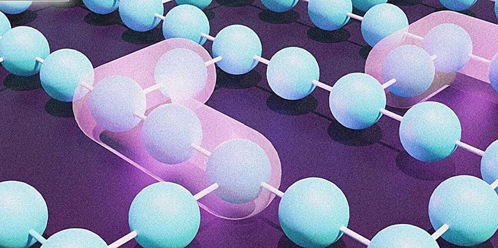
Scientists are exploring various platforms for future large-scale quantum computation. Among the leading contenders, those in which the quantum bits (qubits) are trapped ions stand out for their low-error operation. However, scaling up such platforms to the millions of qubits needed for utility-scale quantum computing is a daunting task. Now Steven Moses at Quantinuum in Colorado and colleagues describe an impressive new trapped-ion quantum computer, the Quantinuum System Model H2, in which they have been able to increase the number of qubits (from 20 to 32) without increasing the error rate [1]. The researchers have put this system through its paces with full component-level testing, a suite of industry-standard benchmark tests, and a set of diverse applications.

In a typical trapped-ion quantum computer, a linear chain of ions is confined by an electric potential using direct-current (dc) and radio-frequency (rf) fields. Whereas the ion-trap apparatus can be at any temperature, the ions themselves need to be laser cooled to near their ground state. Their motion can then be quantized, and the resulting motional modes can be used to entangle any pair of ions in the chain—a requirement for performing quantum operations. However, controlling individual ions in a long chain comes with its own technical difficulties, and it is unlikely that a million qubits—as needed to build a universal, fault-tolerant quantum computer [2]—could be trapped in a single potential.

Dynamic interactive bitwise meta-holography with ultra-high computational and display frame rates

Computer-generated holography (CGH) represents a cutting-edge technology that employs computer algorithms to dynamically reconstruct virtual objects. This technology has found extensive applications across diverse fields such as three-dimensional display, optical information storage and processing, entertainment, and encryption.

Despite the broad application spectrum of CGH, contemporary techniques predominantly rely on projection devices like spatial light modulators (SLMs) and digital micromirror devices (DMDs). These devices inherently face limitations in display capabilities, often resulting in narrow field-of-view and multilevel diffraction in projected images.

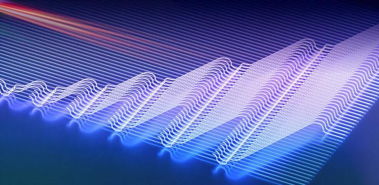
In recent developments, metasurfaces composed of an array of subwavelength nanostructures have demonstrated exceptional capabilities in modulating electromagnetic waves. By introducing abrupt changes to fundamental wave properties like amplitude and phase through nanostructuring at subwavelength scales, metasurfaces enable modulation effects that are challenging to achieve with traditional devices.

Team develops transistors with sliding ferroelectricity based on polarity-switchable molybdenum disulfide

Over the past few years, engineers have been trying to devise alternative hardware designs that would allow a single device to both perform computations and store data. These emerging electronics, known as computing-in-memory devices, could have numerous advantages, including faster speeds and enhanced data analysis capabilities.

To store data safely and retain a , these devices should be based on with advantageous properties and that can be scaled down in terms of thickness. Two-dimensional (2D) semiconductors that exhibit a property known as sliding ferroelectricity have been found to be promising candidates for realizing computing-in-memory, yet attaining the necessary switchable electric polarization in these materials can prove difficult.

Researchers at National Taiwan Normal University, Taiwan Semiconductor Research Institute, National Yang Ming Chiao Tung University and National Cheng Kung University recently devised an effective strategy to achieve a switchable electric polarization in molybdenum disulfide (MoS2). Using this method, outlined in a Nature Electronics paper, they ultimately developed new promising ferroelectric transistors for computing-in-memory applications.

2204.04261 (1).Pdf

Joe McEntee visits the Lawrence Berkeley National Laboratory to learn about QUANT-NET’s plan to create a quantum network tested for distributed quantum computing applications in the US. Joe McEntee visits Lawrence Berkeley National Laboratory (Berkeley Lab) in California to check out progress on the enabling quantum technologies.

Researchers demonstrate the potential of a new quantum material for creating two spintronic technologies

Over the past decade or so, physicists and engineers have been trying to identify new materials that could enable the development of electronic devices that are faster, smaller and more robust. This has become increasingly crucial, as existing technologies are made of materials that are gradually approaching their physical limits.

Antiferromagnetic (AFM) spintronics are devices or components for electronics that couple a flowing current of charge to the ordered spin ‘texture’ of specific materials. In physics, the term spin refers to the intrinsic angular momentum observed in electrons and other particles.

The successful development of AFM spintronics could have very important implications, as it could lead to the creation of devices or components that surpass Moore’s law, a principle first introduced by microchip manufacturer Gordon Earle Moore’s law essentially states that the memory, speed and performance of computers may be expected to double every two years due to the increase in the number of transistors that a microchip can contain.