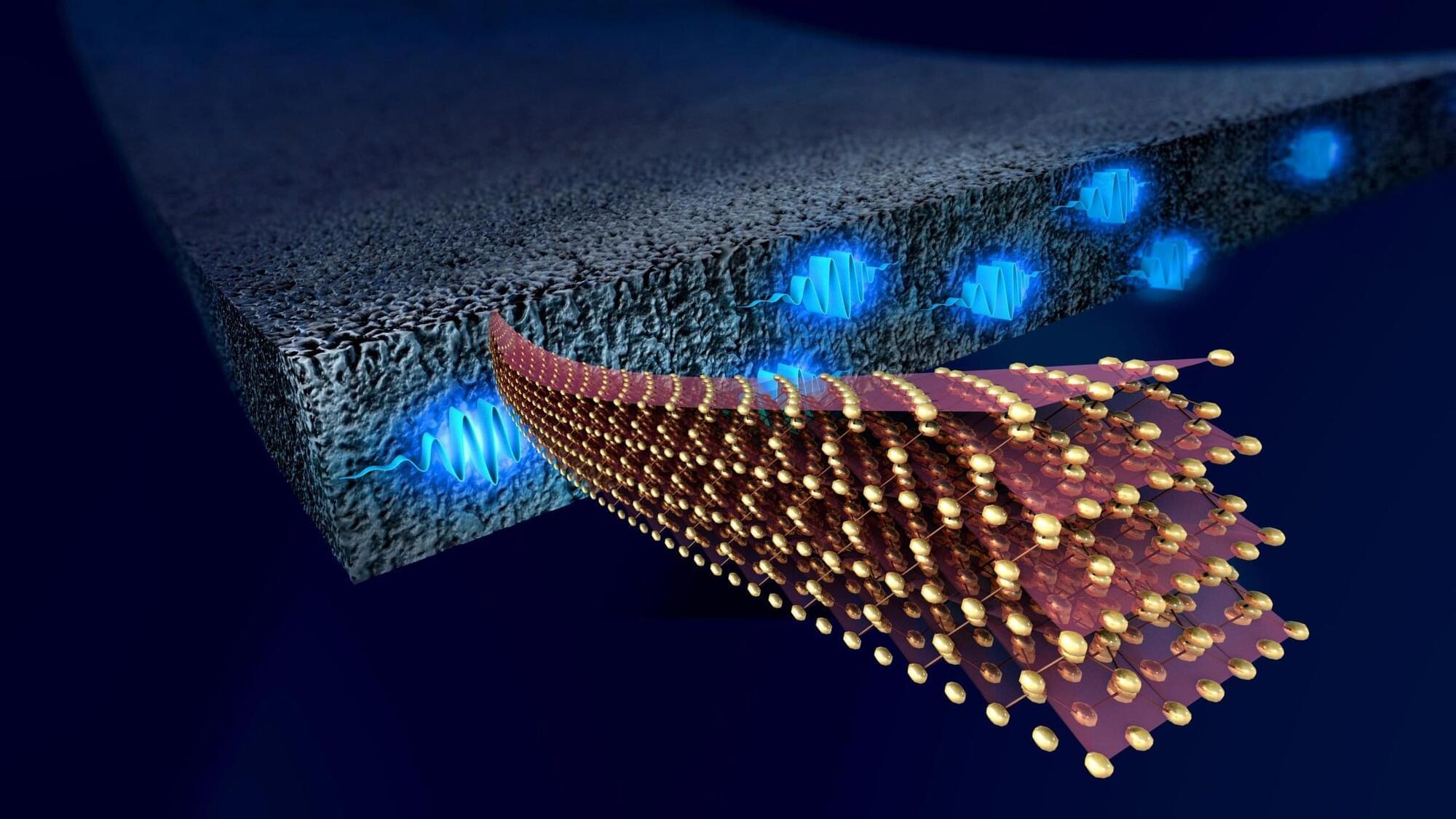
Toggle light / dark theme

The Moon’s Origin Story: A Tale of Collision and Reconstruction

“For the first time we have physical evidence showing us what was happening in the moon’s interior during this critical stage in its evolution, and that’s really exciting,” said Dr. Jeff Andrews-Hanna.


Our Moon has long been hypothesized to have formed from a planet-sized object colliding with the Earth. But, what happened after and how can its unique geologic exterior and interior be explained? This is what a recent study published in Nature Geoscience hopes to address as an international team of researchers led by the Lunar and Planetary Laboratory (LPL) at the University of Arizona used a combination of spacecraft data and computer models to investigate the geologic processes that led to heavier elements being present on the nearside of the Moon, which is constantly facing Earth due to being tidally locked with our planet. This study holds the potential to help researchers better understand the geologic mechanisms behind planetary formation and could lead to gaining greater insight into how rocky planets like Earth and Mars formed.

For the study, the researchers used data from NASA’s GRAIL mission, which was used to map gravitational anomalies on the Moon, and computer models to determine the distribution of ilmenite, a combination of titanium and iron, across the Moon’s nearside and how much sunk into the Moon’s interior during the Moon’s formation and evolution. It has been previously hypothesized that while ilmenite sunk to the Moon’s interior early on, portions of it returned to the surface from volcanism, and the mechanisms behind these events have led scientists puzzled.

Scientists hit a 301 Tbps speed over existing fiber networks

When I was a kid, I went to a science camp, and one of the instructors showed us a few inches of fiber optic cable. I remember thinking it was so neat that you could light it up at one end, and no matter how you twisted the cable, you could see the light come out on the other end. At the time, I thought how useful it might be to send Morse code through it—I was very young. Things have changed a bit since then. Today, UK Aston University researchers sent data at a 301 terabits per second (Tbps) clip over existing fiber networks.

How fast is that? It’s about 1.2 million times faster than the US’ medium fixed broadband speed of 242.48 megabits per second (Mbps). Or, it’s fast enough to deliver 1,800 4K movies to your home in a second. And I thought my recent home internet fiber upgrade to 2 Gigabits per second (Gbps) was impressive!Of course, no one will get 301 Tbps speeds in their home office. In the real world, I know a handful of people with 10 Gbps connections to their houses and many data centers with 40 Gbps local area networks.

Unlocking the Secrets of Eternal Data With Silicon Carbide

Team presents new path to long-term data storage based on atomic-scale defects.

With the development of the internet, social media, and cloud computing, the amount of data created worldwide on a daily basis is skyrocketing. This calls for new technologies that could provide higher storage densities combined with secure long-term data archiving far beyond the capabilities of traditional data storage devices. An international research team led by the Helmholtz-Zentrum Dresden-Rossendorf (HZDR) now proposes a new concept of long-term data storage based on atomic-scale defects in silicon carbide, a semiconducting material. These defects are created by a focused ion beam, providing high spatial resolution, fast writing speed, and low energy for storing a single bit, as the team reports in the journal Advanced Functional Materials.

Latest estimates assume around 330 million terabytes of new data created each day, with 90 percent of the world’s data generated in the last two years alone. If the sheer numbers already suggest the need of advanced data storage technologies, it is by no means the only problem associated to this development. “The limited storage time of current storage media requires data migration within several years to avoid any data loss. Besides of being trapped in perpetual data migration procedures, this substantially increases the energy consumption, because a significant amount of energy is consumed in the process,” says Dr. Georgy Astakhov from the Institute of Ion Beam Physics and Materials Research at HZDR.

Invention Can ‘Shield’ Quantum Computers From Magnetic Interference

PRESS RELEASE — Magnetic Shields Limited (MSL) has invented a lightweight and small-scale magnetic shielding system for cryogenic conditions.

The innovation developed by UK-based MSL in collaboration with the University of Nottingham and quantum computer developer SEEQC will revolutionise quantum computing performance and efficiency. The coil shield also has implications for satellites, where payload weight determines launch costs.

The shield is the first to integrate thin metal coils into magnetic shielding to actively cancel out magnetic field interference in temperatures near absolute zero. It eliminates the need for bulky metal housings.

A physicist uses X-rays to rescue old music recordings

Researchers are developing a technique that uses the special synchrotron X-ray light from the Swiss Light Source SLS to non-destructively digitize recordings from high-value historic audio tapes—including treasures from the Montreux Jazz Festival archive, such as a rare recording of the King of the Blues, B.B. King.

Magnetic tapes have almost completely disappeared from our lives and now only enjoy a nostalgic niche existence. However, significant quantities of these analog are still stored in the archives of sound studios, radio and TV stations, museums, and private collections worldwide. Digitizing these tapes is an ongoing challenge as well as a race against time, as the tapes degrade and eventually become unplayable.

Sebastian Gliga, physicist at PSI and expert in nanomagnetism, and his team are developing a method to non-destructively digitize degraded audio tapes in the highest quality using X-ray light. To achieve this goal, they have been collaborating with the Swiss National Sound Archives, which has produced custom-made reference recordings and provided audio engineering know-how. Now, a partnership with the Montreux Jazz Digital Project will help to further develop and test the method.

The Magnetic Twist: Hybrid Superconductors Unlock Quantum Computing Potential

An international team including researchers from the University of Würzburg has succeeded in creating a special state of superconductivity. This discovery could advance the development of quantum computers.

Superconductors are materials that can conduct electricity without electrical resistance – making them the ideal base material for electronic components in MRI machines, magnetic levitation trains, and even particle accelerators. However, conventional superconductors are easily disturbed by magnetism. An international group of researchers has now succeeded in building a hybrid device consisting of a stable proximitized-superconductor enhanced by magnetism and whose function can be specifically controlled.

They combined the superconductor with a special semiconductor material known as a topological insulator. “Topological insulators are materials that conduct electricity on their surface but not inside. This is due to their unique topological structure, i.e. the special arrangement of the electrons,” explains Professor Charles Gould, a physicist at the Institute for Topological Insulators at the University of Würzburg (JMU). “The exciting thing is that we can equip topological insulators with magnetic atoms so that they can be controlled by a magnet.”

It Is Time To Take Intel Seriously As A Chip Foundry

The third proof point is both the increase in manufacturing capacity investment and the change in how that investment will be managed. With the interest in governments to secure future semiconductor manufacturing for both supply security and economic growth, Mr. Gelsinger went on a spending spree with investment in expanding capacity in Oregon, Ireland, and Israel, as well as six new fabs in Arizona, Ohio, and Germany. Most of the initial investment was made without the promise of government grants, such as the US Chips Act. However, Intel has now secured more than $50B from US and European government incentives, customer commitments starting with its first five customers on the 18A process node, and its financial partners. Intel has also secured an additional $11B loan from the US government and a 25% investment tax credit.

In addition to it’s own investment in fab capacity, Intel is partnering with Tower Semiconductor and UMC, two foundries with long and successful histories. Tower will be investing in new equipment to be installed in Intel’s New Mexico facility for analog products, and UMC will partner with Intel to leverage three of the older Arizona fabs and process nodes, starting with the 12nm, to support applications like industrial IoT, mobile, communications infrastructure, and networking.

The second side of this investment is how current and future capacity will be used. As strictly an IDM, Intel has historically capitalized on its investments in the physical fab structures by retrofitting the fabs after three process nodes, on average. While this allowed for the reuse of the structures and infrastructure, it eliminated support for older process nodes, which are important for many foundry customers. According to Omdia Research, less than 3% of all semiconductors are produced on the latest process nodes. As a result, Intel is shifting from retrofitting fabs for new process nodes to maintaining fabs to support extended life cycles of older process nodes, as shown in the chart below. This requires additional capacity for newer process nodes.

2D magnets could pave the way for green computing

A team of MIT researchers has addressed significant barriers to the practical application of 2D magnetic materials. This innovation will enable the development of the next generation of energy-efficient computers.

The team achieved a notable breakthrough by developing a “van der Waals atomically layered heterostructure” device. The device connects two 2D materials: tungsten ditelluride and iron gallium telluride, a 2D van der Waals magnet.

/* */