The rules about magnetic order may need to be rewritten. Researchers have discovered that chromium selenide (Cr₂Se₃) — traditionally non-magnetic in bulk form — transforms into a magnetic material when reduced to atomically thin layers. This finding contradicts previous theoretical predictions, and opens new possibilities for spintronics applications. This could lead to faster, smaller, and more efficient electronic components for smartphones, data storage, and other essential technologies.
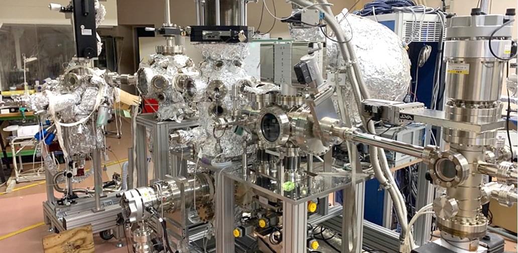
An international research team from Tohoku University, Université de Lorraine (Synchrotron SOLEIL), the National Synchrotron Radiation Research Center (NSRRC), High Energy Accelerator Research Organization, and National Institutes for Quantum Science and Technology successfully grew two-dimensional Cr₂Se₃ thin films on graphene using molecular beam epitaxy. By systematically reducing the thickness from three layers to one layer and analyzing them with high-brightness synchrotron X-rays, the team made a surprising discovery. This finding challenges conventional theoretical predictions that two-dimensional materials cannot maintain magnetic order.
“When we first observed the ferromagnetic behavior in these ultra-thin films, we were genuinely shocked,” explains Professor Takafumi Sato (WPI-AIMR, Tohoku University), the lead researcher. “Conventional theory told us this shouldn’t happen. What’s even more fascinating is that the thinner we made the films, the stronger the magnetic properties became—completely contrary to what we expected.”