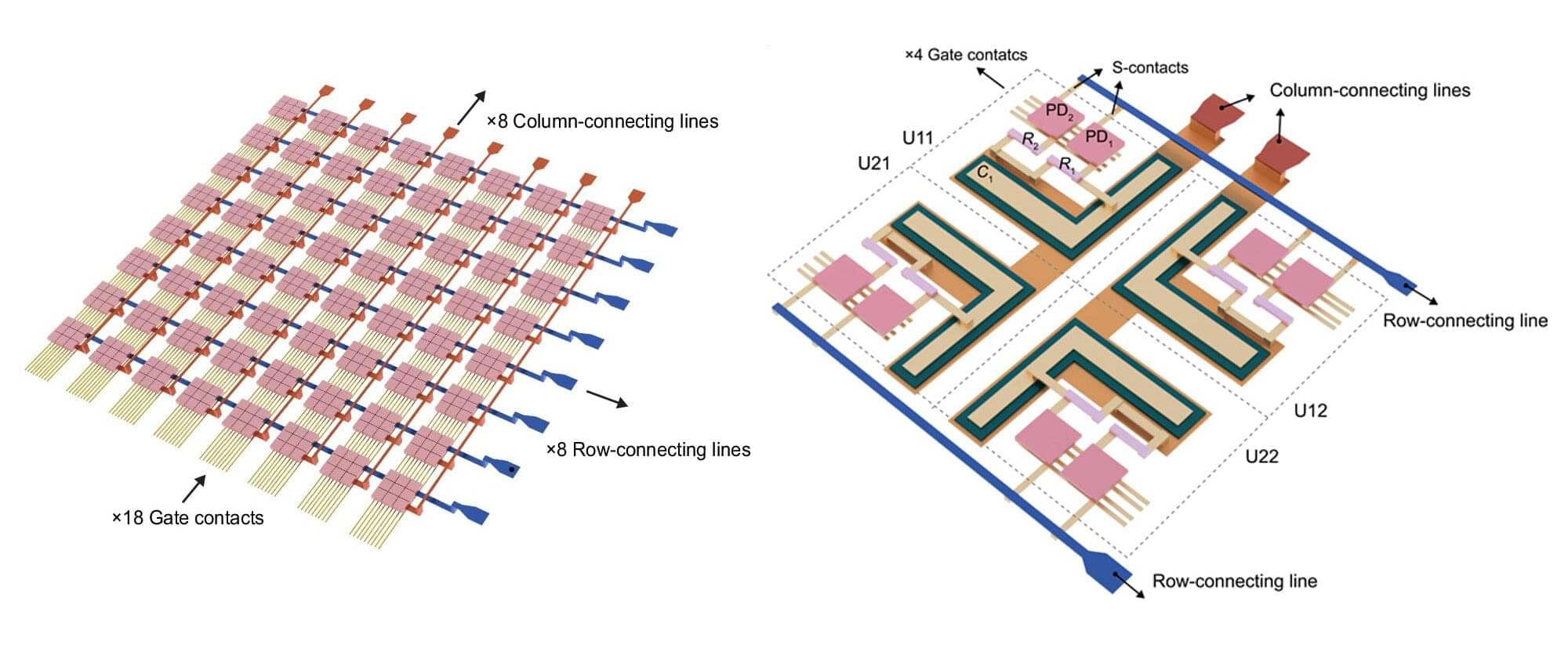
Toggle light / dark theme

This microchip is the size of a grain of sand, and its job is to track data.


Inspired by nature, the latest microchip can dissolve and fly.

About the size of a grain of sand, the chips might be the smallest artificial flying structures yet built — gadgets that could one-day monitor air pollution and the spread of airborne diseases.

Researchers with the Department of Energy’s SLAC National Accelerator Laboratory, Stanford University and the DOE’s Lawrence Berkeley National Laboratory (LBNL) have grown a twisted multilayer crystal structure for the first time and measured the structure’s key properties. The twisted structure could help researchers develop next-generation materials for solar cells, quantum computers, lasers and other devices.

“This structure is something that we have not seen before—it was a huge surprise to me,” said Yi Cui, a professor at Stanford and SLAC and co-author of a paper published in Science describing the work. “A new quantum electronic property could appear within this three-layer twisted structure in future experiments.”

The Framework Laptop 16 is the most customizable laptop we’ve ever seen, with tons of input and port options, and the promise of upgradable graphics. It has a bright screen and solid battery life, but it’s expensive, and you could get something with more performance for the price.


Framework introduces replaceable graphics for the first time, along with customizable keyboards and other accessories.

Year 2021 Biocomputing is the future for the biological singularity because we could control all inputs and outputs of our bodies even evolve them eventually.


A silicon device that can change skin tissue into blood vessels and nerve cells has advanced from prototype to standardized fabrication, meaning it can now be made in a consistent, reproducible way. As reported in Nature Protocols, this work, developed by researchers at the Indiana University School of Medicine, takes the device one step closer to potential use as a treatment for people with a variety of health concerns.

The technology, called tissue nanotransfection, is a non-invasive nanochip device that can reprogram tissue function by applying a harmless electric spark to deliver specific genes in a fraction of a second. In laboratory studies, the device successfully converted into to repair a badly injured leg. The technology is currently being used to reprogram tissue for different kinds of therapies, such as repairing caused by stroke or preventing and reversing nerve damage caused by diabetes.

“This report on how to exactly produce these tissue nanotransfection chips will enable other researchers to participate in this new development in ,” said Chandan Sen, director of the Indiana Center for Regenerative Medicine and Engineering, associate vice president for research and Distinguished Professor at the IU School of Medicine.

A team of researchers headed by Professor Sun Zhong at Peking University recently unveiled an analog hardware approach for real-time compressed sensing recovery. Their findings have been documented in a paper recently published in Science Advances.

In this work, a design based on a resistive memory (also known as memristor) array for performing instantaneous matrix-matrix-vector multiplication (MMVM) is first introduced. Based on this module, then an analog matrix computing circuit that solves compressed sensing (CS) recovery in one step (within a few microseconds) is disclosed.

Kenya has announced that the precious coltan mineral, which is used in the manufacture of cell phones, laptops and other communication gadgets has been found in the country.

Mining and Blue Economy Cabinet Secretary (CS) Salim Mvurya said on Wednesday that adequate deposits of coltan have been found in six counties.

The rare metallic mineral, mostly found in the eastern part of the Democratic Republic of Congo (DRC), is mainly used for the production of electronic goods of mass consumption, such as mobile phones, laptops and videogame consoles, and its discovery in Kenya is set to raise the country’s profile as a mineral exporter.

Tunneling is one of most fundamental processes in quantum mechanics, where the wave packet could traverse a classically insurmountable energy barrier with a certain probability.

On the , effects play an important role in , such as accelerating enzyme catalysis, prompting spontaneous mutations in DNA and triggering olfactory signaling cascades.

Photoelectron tunneling is a key process in light-induced , charge and energy transfer and radiation emission. The size of optoelectronic chips and other devices has been close to the sub-nanometer atomic scale, and the quantum tunneling effects between different channels would be significantly enhanced.

Add a dash of creamer to your morning coffee, and clouds of white liquid will swirl around your cup. But give it a few seconds, and those swirls will disappear, leaving you with an ordinary mug of brown liquid.

Something similar happens in quantum computer chips—devices that tap into the strange properties of the universe at its smallest scales—where information can quickly jumble up, limiting the memory capabilities of these tools.

That doesn’t have to be the case, said Rahul Nandkishore, associate professor of physics at the University of Colorado Boulder.