Background and ObjectivesMultiple sclerosis (MS) is a chronic progressive, demyelinating autoimmune CNS disease. Autoantibodies to the motif P-(SA)-x-(SGA)-R-(SN)-(LRKH) are a class of predictive markers specific to MS that could add to emerging…

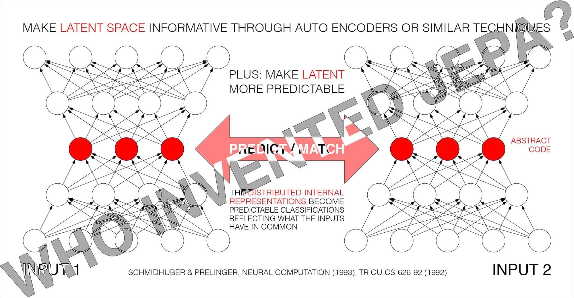
Yann LeCun said:
BREAKING: Schmidhuber claims to have invented JEPA in 1992!
Is anyone surprised?
At some point, when I have nothing better to do, I’ll write a piece about what it means to invent something.
Speaking of which, one day, when I was still in high school, I wrote f(x)=0.
Every theory, every algorithm, is a special case of this (with proper definitions for f and x).
Every technology is a practical application of it.
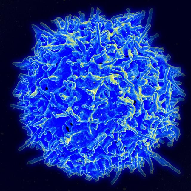
Signaling is fundamental to how cells sense and respond to their environment—but in immune cells, those signals must be precisely amplified to mount an effective defense against invasive threats. New research by immunologists in Germany is shedding light on how that amplification occurs in T cells, revealing a key molecular mechanism that helps trigger immune responses—and may also contribute to inflammatory conditions.
Writing in Science Signaling, researchers at the University Medical Center Hamburg-Eppendorf identified a crucial step in the production of a “second messenger,” an internal signal that relays and amplifies messages received at the cell surface. Because external signaling molecules cannot enter the cell, second messengers translate those cues into powerful intracellular responses.
In T cells, that process depends on NAADP (nicotinic acid adenine dinucleotide phosphate), a molecule that drives calcium (Ca²⁺) signaling—an essential step in T cell activation. Without it, T cells cannot become the effector cells needed to fight serious threats, such as infections or cancer.
Join us as we countdown to launch of Artemis II from historic Launch Complex 39B at NASA Kennedy Space Center in Florida.
#NASA #Artemis #SLS
This coverage is made possible by our amazing community! Consider becoming a The Launch Pad Member and go behind the scenes with early video access, behind the scenes live streams and more!
OUR MISSION:
To inform and inspire the explorers of tomorrow; because we believe that space is better together.
Join our community Discord! / discord.
Website: https://tlpnetwork.com.
Follow us X! / tlpn_official.
Like us on Facebook! / thelaunchpadnetwork.
#Artemis #MoonRocket #Orion #Moon #Rocket #SpaceCoast #NASATV #NASALive
Artemis II Moon Rocket Launch LIVE: NASA’s Artemis II Live Views from Kennedy Space Center, FL | CNBC TV18
LIVE feed from Kennedy Space Center in Florida will provide continuous views of the Artemis II Moon rocket beginning on Thursday, March 19, with rollout from the Vehicle Assembly Building to Launch Pad 39B. NASA Sends Astronauts around the Moon for the first time in 50 years.
Live view of the Artemis II Moon rocket. While the Artemis II launch window opens as early as Wednesday, April 1, the mission management team will assess flight readiness across the spacecraft, launch infrastructure, and the crew and operations teams before selecting a launch date. NASA’s Artemis II mission is scheduled to lift off from Kennedy Space Center on April 1. The two-hour launch window starts at 6:24 p.m. EDT (2224 UTC).
Four astronauts — three from NASA and one from the CSA (Canadian Space Agency) — make up the Artemis II crew:
NASA astronaut Reid Wiseman, Artemis II commander.
NASA astronaut Victor Glover, Artemis II pilot.
NASA astronaut Christina Koch, Artemis II mission specialist.
Canadian Space Agency (CSA) astronaut Jeremy Hansen, Artemis II mission specialist.
After launching into space atop NASA’s Space Launch System (SLS) rocket, the crew will journey around the Moon and back in their Orion spacecraft, named Integrity, on an approximately 10-day mission. Artemis II will be the first crewed flight test of SLS and Orion, testing the technologies we’ll need for long-term lunar exploration and human missions to Mars.
#nasa #artemislaunch #artemis2 #nasaastronauts #rocketlaunch #cnbctv18 #livestream.
NASA Artemis II launch, Artemis II mission, NASA Artemis II crewed mission, Artemis II launch live, Artemis II moon mission, NASA Artemis program, Artemis II astronauts, Orion spacecraft Artemis II, Space Launch System Artemis II, Artemis II lunar flyby, Artemis II mission updates, NASA moon mission 2026, Artemis II launch date, Artemis II spaceflight, NASA crewed moon mission, Artemis II Kennedy Space Center, Artemis II deep space mission, Return to the Moon Artemis II, NASA human spaceflight Artemis II, Artemis II launch coverage.
NASA Artemis moon launch livestream, Artemis moon launch live, NASA Artemis live launch, Artemis mission livestream, NASA moon mission live stream, Artemis launch today live, NASA Artemis rocket launch live, Artemis launch countdown live, NASA Artemis SLS launch live, Artemis Orion spacecraft live stream, NASA Artemis moon mission livestream, Artemis launch Kennedy Space Center live, NASA crewed moon mission live, Artemis lunar mission live coverage, Artemis space launch live updates, NASA Artemis flight livestream, Artemis moon launch live video, NASA Artemis launch webcast, Artemis live launch coverage, Return to the Moon Artemis livestream.
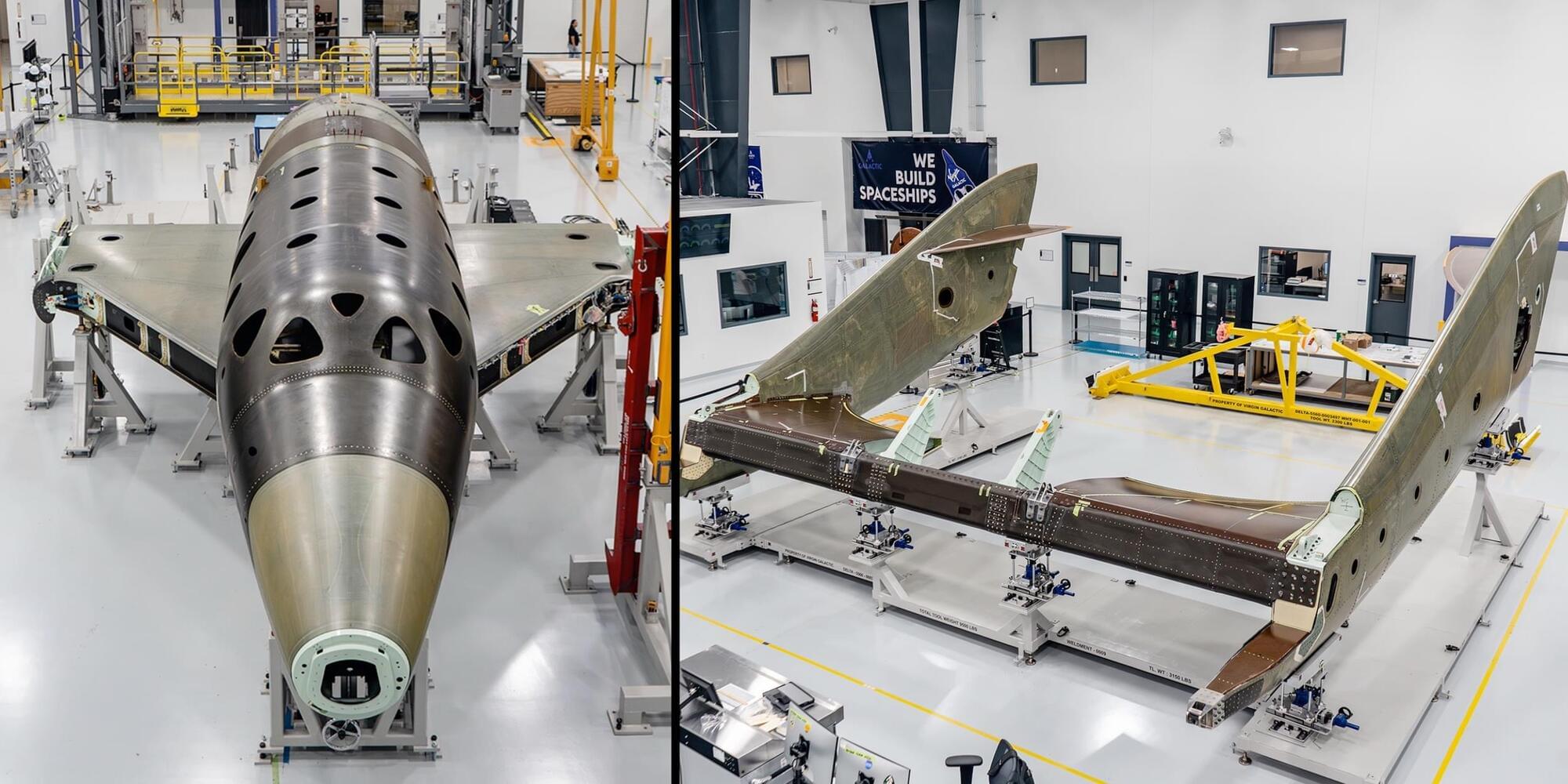
“These spaceflights will be slotted in our manifest immediately after we fly the current members of our founding astronaut community, many of whom have been anticipating their spaceflight for several years,” he said.
The company started ticket sales about two decades ago and says it currently has a backlog of more than 650 customers. In its annual report for 2024, filed in February 2025, the company said it had a backlog of about 700 customers as of the end of 2024.
Virgin Galactic reported $2 million in revenue for 2025 and a net loss of $279 million. It ended the year with $338 million in cash and equivalents on hand.
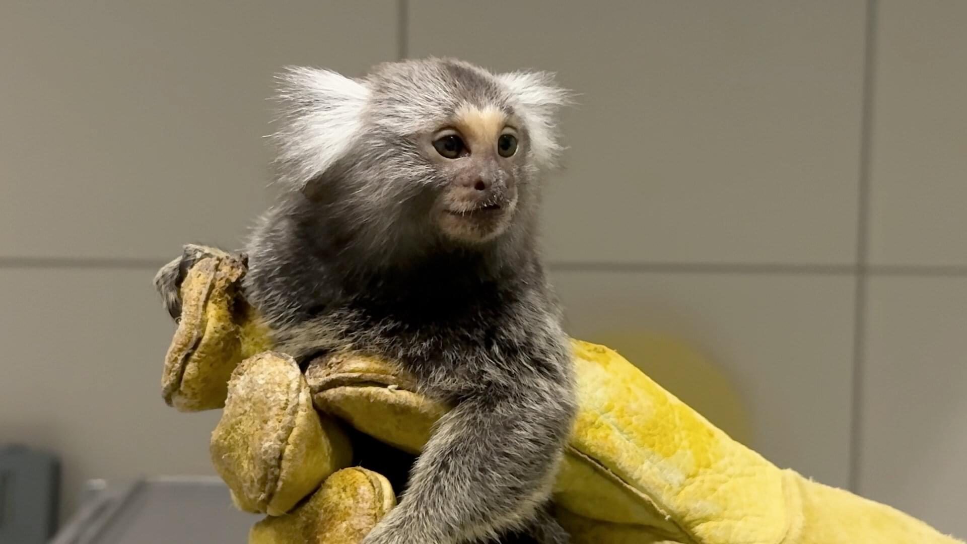
Why are some people unable to hear from birth, even though their inner ear appears intact? One possible cause lies in the so-called OTOF gene. It plays a central role in transmitting sound signals from the hair cells to the auditory nerve. Without this function, acoustic information does not reach the brain.
Researchers from the German Primate Center—Leibniz Institute for Primate Research, the University Medical Center Göttingen, and the Max Planck Institute for Multidisciplinary Sciences have now, for the first time, generated marmosets in which this gene has been knocked out precisely. The animals are healthy and develop normally, but are deaf from birth. This provides the first primate model that realistically replicates key characteristics of human deafness. The results are published in Nature Communications.
Hearing loss is one of the most common congenital sensory disorders in humans. A major cause is a defect in the OTOF gene. This gene ensures that the protein otoferlin is produced in the inner ear. This protein is necessary for sound signals to travel from the hair cells to the auditory nerve. Without it, the ear still functions externally, but the signals do not reach the brain.