Two-dimensional (2D) semiconductors, such as molybdenum disulfide (MoS2), enable unprecedented opportunities to solve the bottleneck of transistor scaling and to build novel logic circuits with faster speeds, lower power consumption, flexibility and transparency, benefiting from their ultra-thin thickness, dangling-bond-free flat surface and excellent gate controllability.
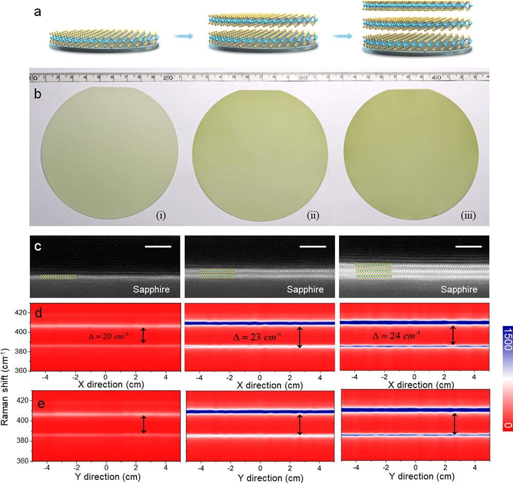
Tremendous efforts have been devoted to exploring the scaled-up potentials of monolayer MoS2, including both wafer-scale synthesis of high-quality materials and large-area devices. For instance, four-inch wafer-scale monolayer MoS2 with large domain sizes (up to ~300 μm) and record-high electronic quality (average field-effect mobility of ~80 cm2·V-1 ·s-1) has already been demonstrated via van der Waals epitaxial growth.
In terms of a further improvement of the electronic quality of the large-scale monolayer MoS2, structural imperfections should be eliminated as much as possible; however, there is not much space left for monolayer MoS2 after ten years of synthesis optimizations in this field. Another key direction is to switch to multilayer MoS2, e.g., bilayers and trilayers, since they have intrinsically higher electronic quality than monolayers and thus are conducive to higher-performance devices and logic circuits. However, due to the fundamental limitation of thermodynamics, it is still a great challenge to realize wafer-scale multilayer MoS2 with high-quality and large-scale uniformity.