Two-dimensional (2D) semiconductors are thin materials (i.e., one-atom thick) with advantageous electronic properties. These materials have proved to be promising for the development of thinner, highly performing electronics, such as fitness trackers and portable devices.
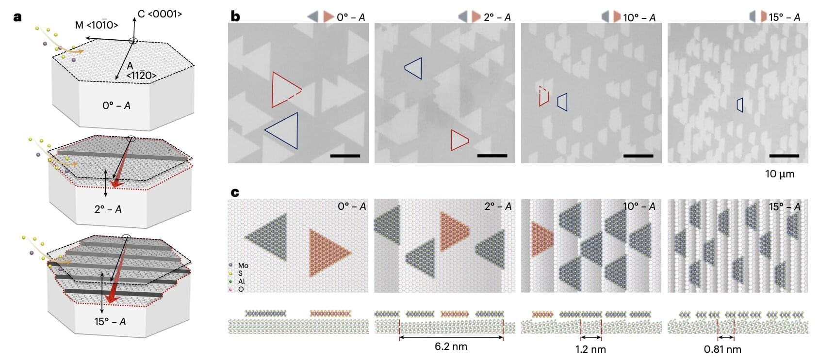
A 2D semiconductor that has attracted particular interest within the electronics community is molybdenum disulfide (MoS₂), a transition-metal dichalcogenide made up of one metal atom and two chalcogen atoms. To build reliable large-area electronics based on MoS₂ layers, engineers need to uniformly grow this material over wafer-scale surfaces, minimizing defects that hinder the performance of devices.
Researchers at the Institute for Basic Science (IBS), Pohang University of Science and Technology (POSTECH) and other institutes recently introduced a new approach to grow single-layer MoS₂ on substrates while maintaining a uniform atomic arrangement. Their approach, outlined in a paper in Nature Electronics, entails a greater control of the process by which small crystal regions merge on a substrate, also known as coalescence.