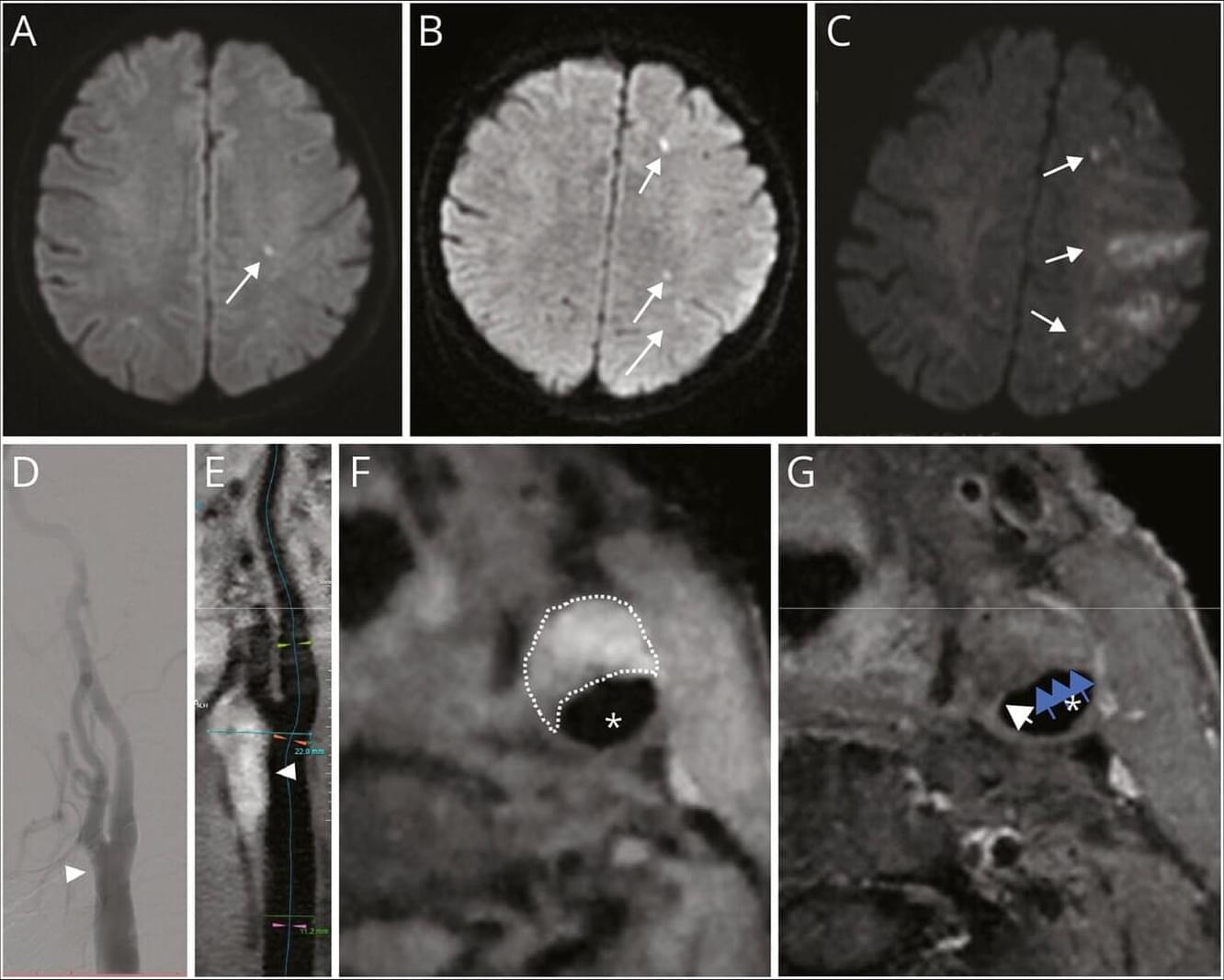
This case provides insight into the high-risk nature of nonstenotic plaques and supports the optimization of stroke risk stratification strategies.

Periodontal disease is a chronic inflammatory condition of the periodontal tissues, encompassing pathologies such as gingivitis and periodontitis. It has been shown that these conditions not only lead to localized inflammation but also have systemic effects on overall health. Recent studies have strongly suggested a link between periodontal disease and chronic systemic diseases, particularly cardiovascular diseases. Among these, endothelial function plays a crucial role in cardiovascular health, and endothelial dysfunction has been reported to contribute to the development of atherosclerosis, hypertension, and coronary artery disease. Endothelial function refers to the ability of endothelial cells to regulate vasodilation and vasoconstriction, primarily through the production and release of nitric oxide.
When ice melts into water, it happens quickly, with the transition from solid to liquid being immediate. However, very thin materials do not adhere to these rules. Instead, an unusual state between solid and liquid arises: the hexatic phase. Researchers at the University of Vienna have now succeeded in directly observing this exotic phase in an atomically thin crystal.
Using state-of-the-art electron microscopy and neural networks, they filmed a silver iodide crystal protected by graphene as it melted. Ultra-thin, two-dimensional materials enabled researchers to directly observe atomic-scale melting processes. The new findings significantly advance the understanding of these phase transitions. Surprisingly, the observations contradict previous predictions—a result now published in Science.
The sudden transition in melting ice is typical of the melting behavior of all three-dimensional materials, from metals and minerals to frozen drinks. However, when a material becomes so thin that it is practically two-dimensional, the rules of melting change dramatically. Between the solid and liquid phases, a new, exotic intermediate phase of matter can arise, known as the “hexatic phase.”

Neutron stars are ultra-dense star remnants made up primarily of nucleons (i.e., protons and neutrons). Over the course of millions of years, these stars progressively cool down, radiating heat into space.
The cooling process of neutron stars could be a promising testbed for various hypothetical particles, including so-called scalar particles. These are particles that do not possess a spin and that, according to some theoretical predictions, could couple to nucleons.
Scalar particles are hypothesized to violate two fundamental laws of gravity, known as the equivalence principle and the inverse-square law. Their observation could thus greatly enrich the present understanding of the universe and its underlying physical forces.
Astronomers have captured images of two stellar explosions—known as novae—within days of their eruption and in unprecedented detail. The breakthrough provides direct evidence that these explosions are more complex than previously thought, with multiple outflows of material and, in some cases, dramatic delays in the ejection process.
The international study, published in the journal Nature Astronomy, used a cutting-edge technique called interferometry at the Center for High Angular Resolution Astronomy (CHARA Array) in California. This approach allowed scientists to combine the light from multiple telescopes, achieving the sharp resolution needed to directly image the rapidly evolving explosions.
“The images give us a close-up view of how material is ejected away from the star during the explosion,” said Georgia State’s Gail Schaefer, director of the CHARA Array. “Catching these transient events requires flexibility to adapt our nighttime schedule as new targets of opportunity are discovered.”
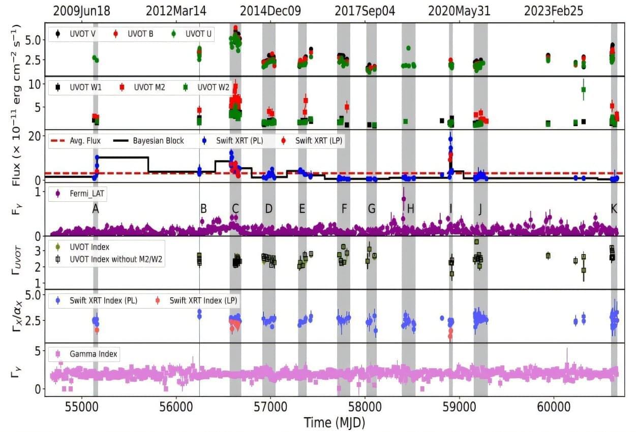
Using NASA’s Swift and Fermi space telescopes, Indian astronomers have conducted a long-term multiwavelength study of a nearby blazar designated TXS 0518+211. Results of the study, published Nov. 26 on the arXiv pre-print server, reveal the complex nature of this object.
Blazars are very compact quasi-stellar objects (quasars) associated with supermassive black holes (SMBHs) at the centers of active, giant elliptical galaxies. They are the most luminous and extreme subclass of active galactic nuclei (AGNs). The characteristic features of blazars are highly collimated relativistic jets pointed almost exactly toward Earth.
Blazars are usually divided by astronomers into two classes, based on their optical emission properties: flat-spectrum radio quasars (FSRQs) that feature prominent and broad optical emission lines, and BL Lacertae objects (BL Lacs), which do not.
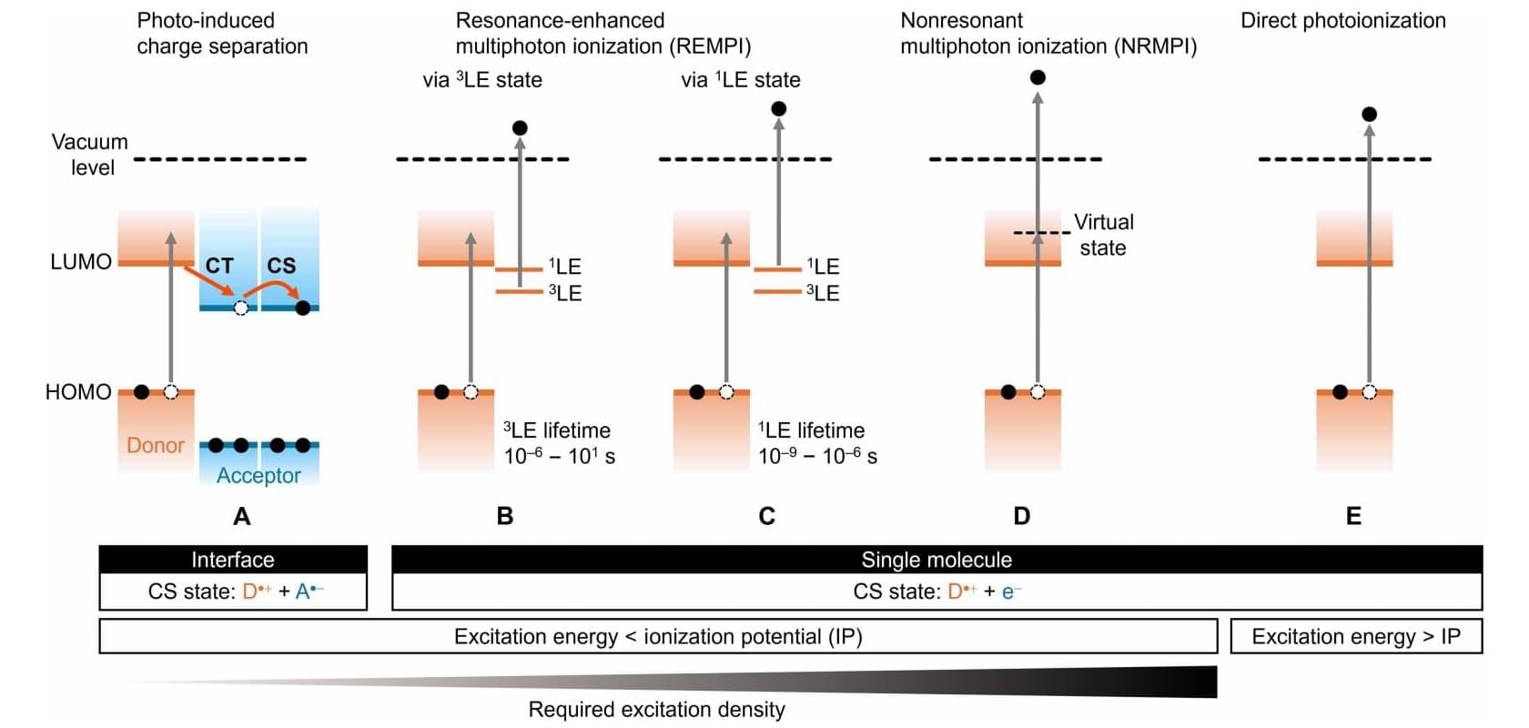
Why does plastic turn brittle and paint fade when exposed to the sun for long periods? Scientists have long known that such organic photodegradation occurs due to the sun’s energy generating free radicals: molecules that have lost an electron to sunlight-induced ionization and have been left with an unpaired one, making them very eager to react with other molecules in the environment. However, the exact mechanisms for how and why the energy from the sun’s photons get stored and released in the materials over very long periods have eluded empirical evidence.
The problem lies in the timeframe. While scientists have access to extremely sophisticated spectroscopy equipment capable of measuring the energy levels of individual electrons at femtosecond to millisecond scales in organic materials, they have paid little attention to time scales beyond seconds—and these are processes that can take years.
As such, slow, transient charge accumulation has presented a disappointing data gap in both applied and theoretical optics. But now, researchers from the Organic Optoelectronics Unit at the Okinawa Institute of Science and Technology (OIST) have addressed this challenge with a new methodology that detects these faint signals. Their findings are published in Science Advances.
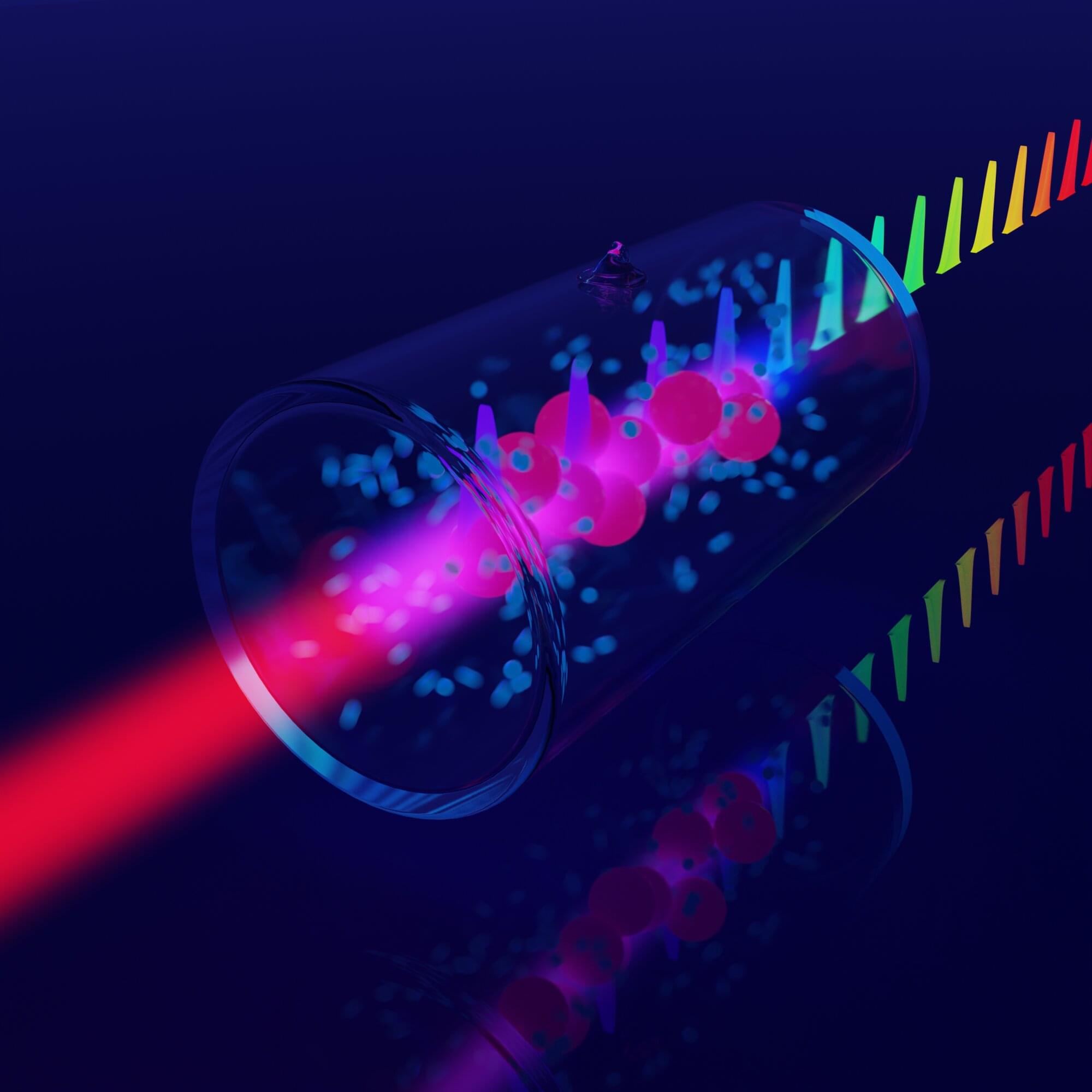
A team from the Faculty of Physics and the Center for Quantum Optica l Technologies at the Center of New Technologies, University of Warsaw has developed a new method for measuring elusive terahertz signals using a “quantum antenna.”
The authors of the work utilized a novel setup for radio wave detection with Rydberg atoms to not only detect but also precisely calibrate a so-called frequency comb in the terahertz band. This band was until recently a white spot in the electromagnetic spectrum, and the solution described in the journal Optica paves the way for ultrasensitive spectroscopy and a new generation of quantum sensors operating at room temperature.
Terahertz (THz) radiation, being part of the electromagnetic spectrum, lies at the boundary of electronics and optics, positioned between microwaves (used, for example, in Wi-Fi) and infrared.
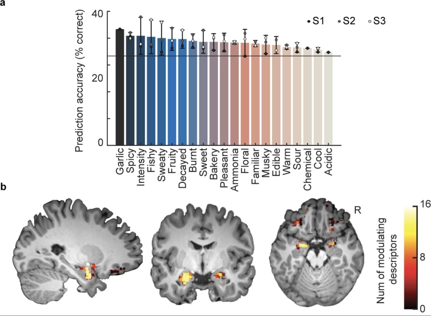
Humans and other animals actively sense their surrounding environment. This entails the deliberate adjustment of motor behavior involved in sensory sampling (i.e., movements of the eyes, ears and hands) in line with the stimulus information.
When it comes to the sense of smell, the principal motor behavior that supports active sensing is the sniff, which entails brief inhalations aimed at pulling odor molecules into the nasal cavity. So far, the extent to which sniffing behaviors can be influenced and adapted based on the odors that one is smelling has remained unknown.
Researchers at Northwestern University recently carried out a study aimed at exploring this possibility. Their findings, published in Nature Human Behavior, suggest that people’s sniffing patterns are continuously shaped by what they are smelling and carry detailed information about specific odors.
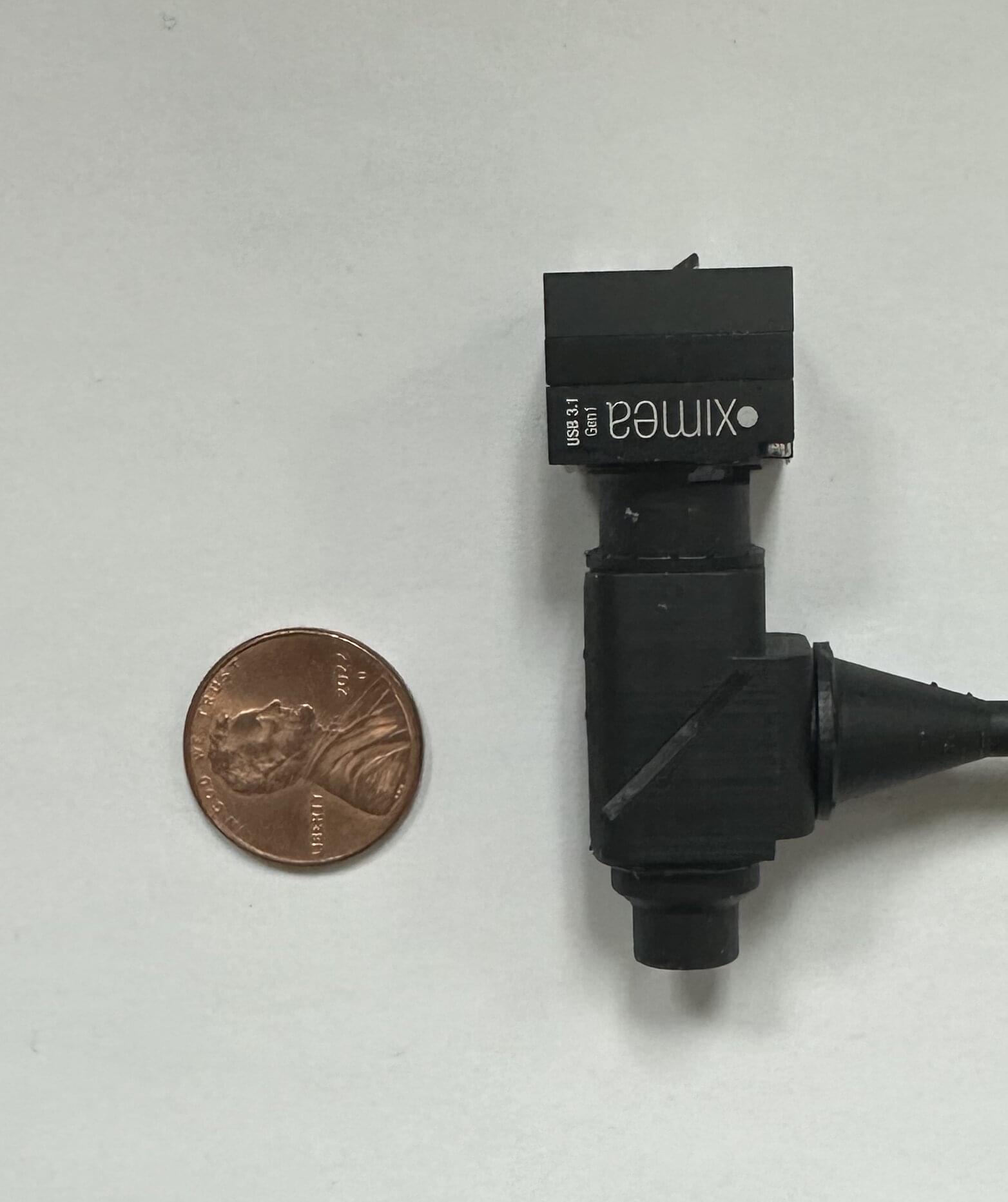
Researchers have built a tiny, lightweight microscope that captures neuron activity with unprecedented speed that can be used in freely moving animals. The new tool could give scientists a more complete view of how brain cells process information during natural behavior.
The microscope is designed to image genetically encoded voltage indicators —fluorescent dyes that rapidly change brightness when a neuron fires—through a small window in the skull while the animal is awake.
“Unlike most miniature microscopes that track slower calcium signals, ours captures electrical spikes at hundreds of frames per second,” said Emily Gibson from the University of Colorado Anschutz Medical Campus. “This makes it possible to capture the moment a neuron fires as well as the quieter signals that build up inside neurons before firing.”