AstraZeneca and Daiichi Sankyo have initiated DESTINY-Endometrial02, a global phase 3 trial evaluating fam-trastuzumab deruxtecan-nxki (T-DXd; Enhertu) as an adjuvant treatment for patients with HER2-expressing endometrial cancer.

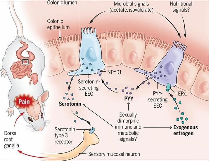
A previously unrecognized estrogen-dependent signaling pathway in the gut regulates visceral pain sensitivity in mice, according to a new Science study. The findings provide a pathway toward targeted therapeutic strategies.
Learn more in a new Science Perspective.
Estrogen tunes a cross-talk between hormone-secreting cells in the mouse gut to regulate visceral pain.
Amélie Joly and Irene Miguel-Aliaga Authors Info & Affiliations
Science
Vol 390, Issue 6779
Copyright © 2025 Science Tech Updates — Keep up-to-date with latest science, astronomy and medical news and research.
Designed by hCG, thanks to: sky3ds, ee signal boosters and HcG Injections
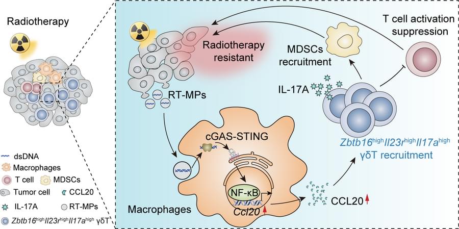
Chao Wan & team show the mechanism by which gamma delta T cells mediate radioresistance, highlighting IL-17 signaling & CCL20 as potential targets for enhancing radiosensitivity:
The figure reflects tumor growth and survival for lung cancer-bearing mice.
1Cancer Center, Union Hospital, Tongji Medical College and.
2Institute of Radiation Oncology, Union Hospital, Tongji Medical College, Huazhong University of Science and Technology, Wuhan, China.
3Hubei Key Laboratory of Precision Radiation Oncology, Wuhan, China.
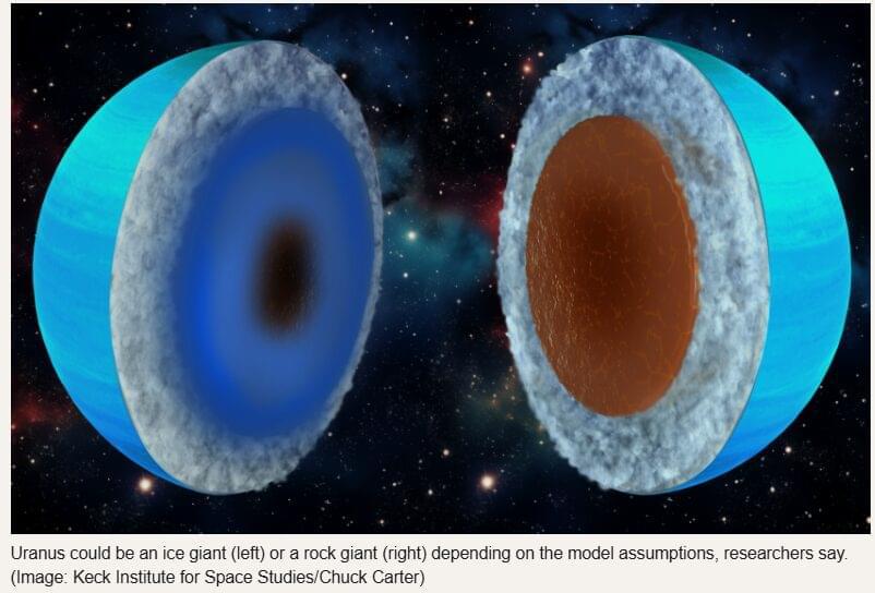
Uranus and Neptune may not be the icy worlds we’ve long imagined. A new Swiss-led study uses innovative hybrid modeling to reveal that these planets could just as easily be dominated by rock as by water-rich ices. The findings also help explain their bizarre, multi-poled magnetic fields and open the door to a wider range of possible interior structures. But major uncertainties remain, and only future space missions will The Solar System is commonly grouped by planetary composition: four rocky terrestrial planets (Mercury, Venus, Earth and Mars), two massive gas giants (Jupiter and Saturn), and a pair of ice giants (Uranus and Neptune). However, new research from a scientific team at the University of Zurich (UZH) suggests that Uranus and Neptune may contain far more rock than previously assumed. The study does not argue that these planets must be either water-rich or rock-rich. Instead, it questions the long-standing idea that an ice-heavy interior is the only conclusion supported by available data. This broader interpretation also aligns with the finding that Pluto, a dwarf planet, is dominated by rock.
To better understand what lies inside Uranus and Neptune, the researchers created a specialized simulation technique. “The ice giant classification is oversimplified as Uranus and Neptune are still poorly understood,” says Luca Morf, PhD student at the University of Zurich and lead author of the work. “Models based on physics were too assumption-heavy, while empirical models are too simplistic. We combined both approaches to get interior models that are both “agnostic” or unbiased and yet, are physically consistent.”
The process begins with a randomly generated density profile representing the interior of each planet. The team then determines the gravitational field that would match observational measurements and uses that information to infer the possible composition. The cycle is repeated until the model best fits all available data.

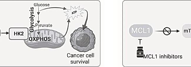
A study by the Mildred Scheel Early Career Center group led by Dr. Mohamed Elgendy at the TUD Faculty of Medicine provides fundamental insights into cancer biology. Published in Nature Communications, the study shows for the first time that the protein MCL1 not only inhibits programmed cell death, but also plays a central role in tumor metabolism.
The researchers have succeeded in tracing two classic hallmarks of cancer—the evasion of apoptosis (a form of programmed cell death) and the dysregulation of energy metabolism—back to a common molecular mechanism.
The study focuses on the protein MCL1, which is strongly overexpressed in many tumor types and has previously been considered primarily an anti-apoptotic factor of the Bcl-2 protein family.

One of the main proteins that contributes to Alzheimer’s disease is called phospho-tau (p-tau). When p-tau gets too many phosphate groups attached to it (a process called hyperphosphorylation), it starts to stick together and form clumps called “tangles” inside of brain nerve cells.
A new study by Mass General Brigham investigators shows that tau hyperphosphorylation may be a consequence of an antiviral response that protects the brain from infection. Results are published in Nature Neuroscience.
“As a geneticist, I always wondered why humans had evolved gene mutations predisposing to Alzheimer’s disease,” said senior author Rudolph Tanzi, Ph.D., Director of the McCance Center for Brain Health and Genetics and Aging Research Unit in the Mass General Brigham Department of Neurology.
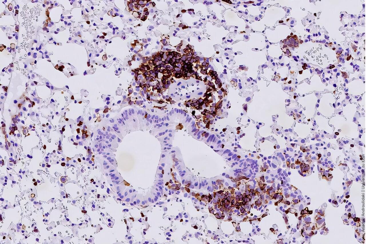
Small cell lung cancer (SCLC) is one of the most aggressive forms of lung cancer, with a five-year survival rate of only 5%. Despite this poor prognosis, SCLC is initially highly responsive to chemotherapy. However, patients typically relapse and experience very rapid disease progression. Current research into the biological mechanisms behind SCLC remains essential in order to prolong treatment responses, overcome relapse and, ultimately, improve long-term patient outcomes.
A research team led by Professor Dr. Silvia von Karstedt (Translational Genomics, CECAD Cluster of Excellence on Aging Research, and Center for Molecular Medicine Cologne—CMMC) has discovered a novel mechanism used by this type of cancer that helps explain its aggressive nature. The study titled “Lack of Caspase 8 Directs Neuronal Progenitor-like reprogramming and Small Cell Lung Cancer Progression” is published in Nature Communications.