Toggle light / dark theme

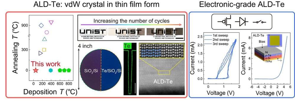
A research team, led by Professor Joonki Suh in the Department of Materials Science and Engineering and the Graduate School of Semiconductor Materials and Devices Engineering at UNIST, has made a significant breakthrough in thin film deposition technology. By employing an innovative atomic layer deposition (ALD) process, Professor Seo successfully achieved regular arrangement of tellurium (Te) atoms at low temperatures as low as 50 degrees Celsius.

The ALD method is a cutting-edge thin film process that enables precise stacking of semiconductor materials at the atomic layer level on three-dimensional structures—even at low process temperatures. However, traditional application to next-generation semiconductors requires high processing temperatures above 250 degrees Celsius and additional heat treatment exceeding 450 degrees Celsius.

In this research, the UNIST team applied ALD to monoelemental van der Waals tellurium—a material under extensive investigation for its potential applications in and thermoelectric materials.

Combinatorial optimization problems (COPs) have applications in many different fields such as logistics, supply chain management, machine learning, material design and drug discovery, among others, for finding the optimal solution to complex problems. These problems are usually very computationally intensive using classical computers and thus solving COPs using quantum computers has attracted significant attention from both academia and industry.

Over the past decade, organic luminescent materials have been recognized by academia and industry alike as promising components for light, flexible and versatile optoelectronic devices such as OLED displays. However, it is a challenge to find suitably efficient materials.

To address this challenge, a joint research team has developed a novel approach combining a machine learning model with quantum-classical computational molecular design to accelerate the discovery of efficient OLED emitters. This research was published May 17 in Intelligent Computing.

The optimal OLED emitter discovered by the authors using this “hybrid quantum-classical procedure” is a deuterated derivative of Alq3 and is both extremely efficient at emitting light and synthesizable.

A research team from City University of Hong Kong (CityU) recently successfully achieved lattice-mismatch-free construction of III-V/chalcogenide core-shell heterostructure nanowires for electronic and optoelectronic applications. This breakthrough addresses crucial technological challenges related to the lattice mismatch problem in the growth of high-quality heterostructure semiconductors, leading to enhanced carrier transport and photoelectric properties.

Nanoscale transistors are in demand for efficient digital circuits, and biasing of each device is critical. These stringent biasing conditions can be relaxed by obtaining precise values of the threshold voltages of the transistor. This leads to more tolerant logic states to the electrical noise.

To meet the requirements of reduced , CMOS field-effect transistors (FETs) are fabricated such that they operate in enhancement (E) mode, i.e., there are no free charge carriers in the channel at zero gate . On the other hand, depletion (D) mode transistors have higher currents than enhancement mode due to ample charge carrier density.

In contrast to switching applications of FET, for high-frequency applications, off-state of FET is not a compulsory requirement. In fact, the presence of a channel at zero gate bias is advantageous to obtain high transconductance at lower voltages. For Si FETs, the enhancement or depletion modes were determined at the fabrication step of ion implantation doping. However, it is challenging to implement this solution for the new generation of thin materials like organic semiconductors and 2D materials.

Related: Scientists find ‘ghost particles’ spewing from our Milky Way galaxy in landmark discovery (video)

“Because like-charged objects in a vacuum are expected to repel regardless of whether the sign of the charge they carry is positive or negative, the expectation is that like-charged particles in solution must also monotonically repel,” the researchers wrote in the paper.

To test the assumption, the researchers placed charged silica microparticles (measuring just 0.0002 inch, or 5 micrometers, wide — a fraction of the width of a human hair) inside water or one of two types of alcohol. By tracking the charges with a microscope, the team established that, inside water, the positively charged particles pushed themselves away from each other in accordance with Coulomb’s law.