Researchers at IMDEA Materials Institute have developed a pioneering method to assemble silicon nanowires into ordered, macroscopic networks: a key step toward expanding their industrial applications.


Stress is a very real factor in the structure of our universe. Not the kind of stress that students experience when taking a test, but rather the physical stresses that affect everyday objects. Consider the stress that heavy vehicles exert on a bridge as they cross over it—it’s essential that engineers understand and consider this factor when designing new trestles. Or consider the stresses that a star experiences—this internal factor influences everything from its shine to its lifetime.
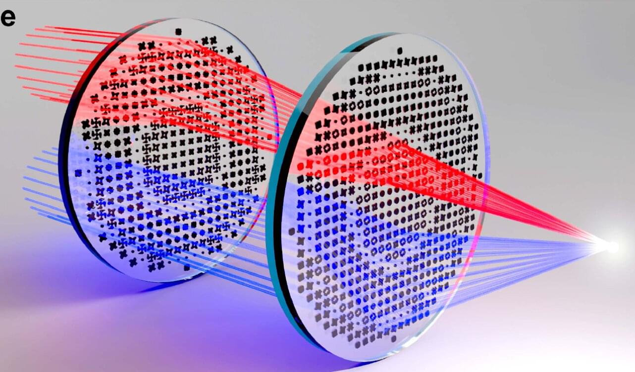
A new approach to manufacturing multicolor lenses could inspire a new generation of tiny, cheap, and powerful optics for portable devices such as phones and drones.
The design uses layers of metamaterials to simultaneously focus a range of wavelengths from an unpolarized source and over a large diameter, overcoming a major limitation of metalenses, said the first author of the paper reporting the design, Joshua Jordaan, from the Research School of Physics at the Australian National University and the ARC Center of Excellence for Transformative Meta-Optical Systems (TMOS).
“Our design has a lot of nice features that make it applicable to practical devices.”
Relaying a message from point A to B can be as simple as flashing a thumbs-up at a stranger in an intersection, signaling them to proceed—nonverbal, clear, and universally understood. But light-based communication is rarely that straightforward.
Photons, tiny particles of light, are fragile and unpredictable. Unlike electrons, which must be conserved in circuits, photons can scatter, split, merge into different colors, or be absorbed, meaning that the number of photons in a system isn’t fixed, even while the energy they carry remains the same. This makes guiding them through fiber optics or photonic chips —optical mazes—far trickier than steering electrons through copper wires, because light signals can scatter into dead ends or vanish before reaching their destination.
Engineers often respond by obsessively refining every imperfection, polishing the maze to perfection. However, this approach can be exhausting and never fully addresses these limitations.
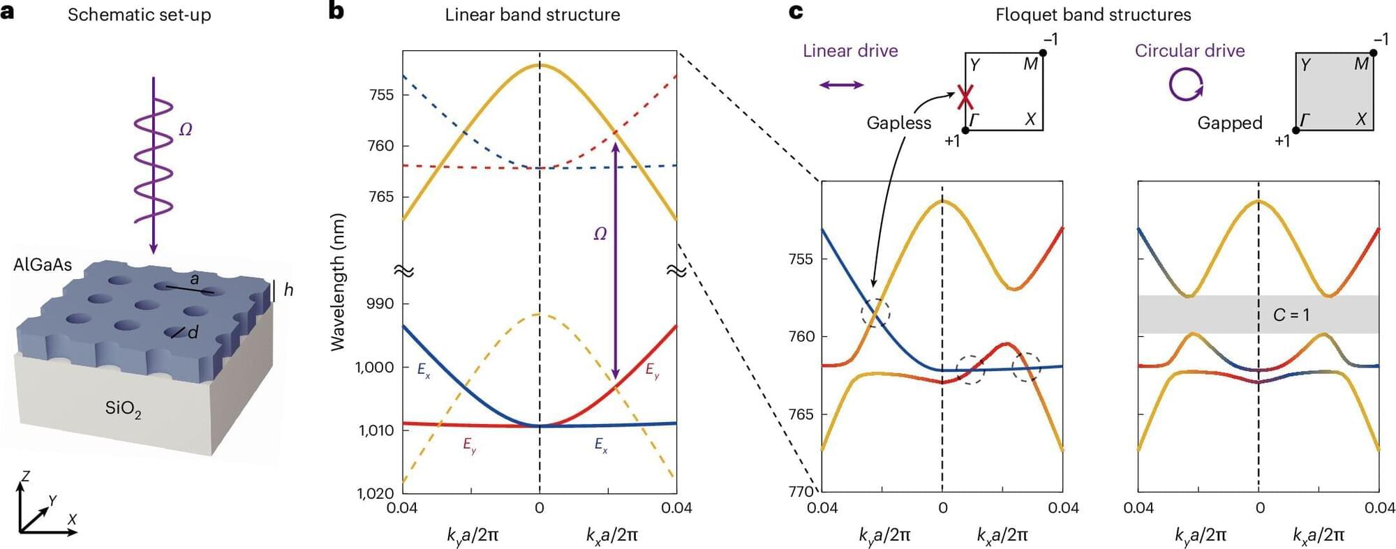
A NIMS research team has developed a magnetic tunnel junction (MTJ) featuring a tunnel barrier made of a high-entropy oxide composed of multiple metallic elements. This MTJ simultaneously demonstrated stronger perpendicular magnetization, a higher tunnel magnetoresistance (TMR) ratio (i.e., the relative change in electrical resistance when the magnetization directions of the two ferromagnetic layers switch between parallel and antiparallel alignments) and lower electrical resistance.
These properties may contribute to the development of smaller, higher-capacity and higher-performance hard disk drives (HDDs) and magnetoresistive random access memory (MRAM).
This research is published in Materials Today.


