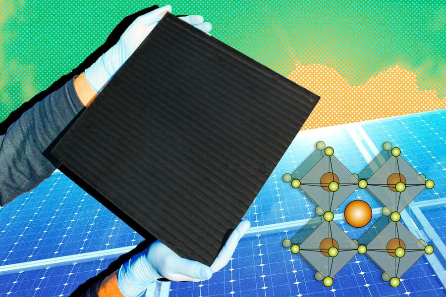
Cloudy days pose a real problem for solar panels. But a new innovation can convert UV light to energy—even if the sun isn’t shining.
Category: solar power – Page 86
When light falls on a material, such as a green leaf or the retina, certain molecules transport energy and charge. This ultimately leads to the separation of charges and the generation of electricity. Molecular funnels, so-called conical intersections, ensure that this transport is highly efficient and directed.
An international team of physicists has now observed that such conical intersections also ensure a directed energy transport between neighboring molecules of a nanomaterial. Theoretical simulations have confirmed the experimental results. Until now, scientists had observed this phenomenon only within one molecule. In the long term, the results could help to develop more efficient nanomaterials for organic solar cells, for example. The study, led by Antonietta De Sio, University of Oldenburg, and Thomas Frauenheim, University of Bremen, Germany, was published in the current issue of the scientific journal Nature Nanotechnology.
Photochemical processes play a major role in nature and in technology: When molecules absorb light, their electrons transit to an excited state. This transition triggers extremely fast molecular switching processes. In the human eye, for example, the molecule rhodopsin rotates in a certain way after absorbing light and thus ultimately triggers an electrical signal—the most elementary step in the visual process.
Solar power stations in space that beam ‘emission-free electricity’ down to Earth could soon be a reality thanks to a UK government funded project.
Above the Earth there are no clouds and no day or night that could obstruct the sun’s ray – making a space solar station a constant zero carbon power source.
The UK government commissioned new research into the concept of space-based solar power (SBSP) stations as a way to meet the Earth’s growing energy needs.
A team of physicists from the University of Konstanz and Ludwig-Maximilians-Universität München in Germany have achieved attosecond time resolution in a transmission electron microscope by combining it with a continuous-wave laser—offering new insights into light-matter interactions.
Electron microscopes provide deep insight into the smallest details of matter and can reveal, for example, the atomic configuration of materials, the structure of proteins or the shape of virus particles. However, most materials in nature are not static and rather interact, move and reshape all the time. One of the most common phenomena is the interaction between light and matter, which is ubiquitous in plants as well as in optical components, solar cells, displays or lasers. These interactions—which are defined by electrons being moved around by the field cycles of a light wave—happen at ultrafast time scales of femtoseconds (10-15 seconds) or even attoseconds (10-18 seconds, a billionth of a billionth of a second). While ultrafast electron microscopy can provide some insight into femtosecond processes, it has not been possible, until now, to visualize the reaction dynamics of light and matter occurring at attosecond speeds.
Now, a team of physicists from the University of Konstanz and Ludwig-Maximilians-Universität München have succeeded in combining a transmission electron microscope with a continuous-wave laser to create a prototypical attosecond electron microscope (A-TEM). The results are reported in the latest issue of Science Advances.
Nanographene is a material that could radically improve solar cells, fuel cells, LEDs and more. Typically, the synthesis of this material has been imprecise and difficult to control. For the first time, researchers have discovered a simple way to gain precise control over the fabrication of nanographene. In doing so, they have shed light on the previously unclear chemical processes involved in nanographene production.
Graphene, one-atom-thick sheets of carbon molecules, could revolutionize future technology. Units of graphene are known as nanographene; these are tailored to specific functions, and as such, their fabrication process is more complicated than that of generic graphene. Nanographene is made by selectively removing hydrogen atoms from organic molecules of carbon and hydrogen, a process called dehydrogenation.
“Dehydrogenation takes place on a metal surface such as that of silver, gold or copper, which acts as a catalyst, a material that enables or speeds up a reaction,” said Assistant Professor Akitoshi Shiotari from the Department of Advanced Materials Science. “However, this surface is large relative to the target organic molecules. This contributes to the difficulty in crafting specific nanographene formations. We needed a better understanding of the catalytic process and a more precise way to control it.”
A Chinese team has demonstrated a prototype of a microwave plasma thruster capable of working in the Earth’s atmosphere and producing thrust with an efficiency comparable to the jet engines you’d find on modern airliners – under laboratory conditions.
Plasma thrusters are already operational on spacecraft as a means of solar-electric locomotion, using xenon plasma, but such things are no use in the Earth’s atmosphere, as accelerated xenon ions lose most of their thrust force to friction against the air. Not to mention, they only make a small amount of thrust in the first place.
This design, conceived and built by a team at the Institute of Technical Sciences at Wuhan University, uses only air and electricity, and appears to produce an impressive push that may see it become relevant to electric aircraft applications.
It seems solar power is really benefiting these chicken farmers from Australia. It allows them to slash their electricity bill.
This 10-million-bird chicken farm has slashed its power bill and reduced its CO2 emissions by 1,500 tonnes after installing one of agriculture’s most extensive solar and battery systems.
This is one of four blogs in a series examining current challenges and opportunities for recycling of clean energy technologies. Please see the introductory post, as well as other entries on solar panels and wind turbines.
us department of energy[ caption] courtesy union concerned scientists. by james gignac, lead midwest energy analyst this is one four blogs in a series examining current challenges and opportunities for recycling clean technologies. please see the introductory post, as well other entries on solar panels and wind turbines. special thanks to jessica garcia, ucs’s=
Well, at least they’re having fun with it.
Most sun oriented homesteads adjust their sunlight based exhibits in lines and segments to shape a matrix.
Another sun based force plant in Datong, China, be that as it may, chose to have some good times with its structure. China Dealers New Vitality Gathering, one of the nation’s biggest clean vitality administrators, fabricated a 248-section of land sun powered ranch looking like a mammoth panda.
Ultra high-res displays for gadgets and tv sets may be coming. 😃
By expanding on existing designs for electrodes of ultra-thin solar panels, Stanford researchers and collaborators in Korea have developed a new architecture for OLED—organic light-emitting diode—displays that could enable televisions, smartphones and virtual or augmented reality devices with resolutions of up to 10,000 pixels per inch (PPI). (For comparison, the resolutions of new smartphones are around 400 to 500 PPI.)
Such high-pixel-density displays will be able to provide stunning images with true-to-life detail—something that will be even more important for headset displays designed to sit just centimeters from our faces.
The advance is based on research by Stanford University materials scientist Mark Brongersma in collaboration with the Samsung Advanced Institute of Technology (SAIT). Brongersma was initially put on this research path because he wanted to create an ultra-thin solar panel design.